GATE 2023 EC Paper: Worked Solutions to All 65 Questions
All 65 questions of the GATE 2023 EC paper (IIT Kanpur), in paper order. Try each one, then open its answer: the official answer from the answer key and a worked solution. Every answer matches the key, and every numerical answer was recomputed from the question's values.
Q.1
General Aptitude1 markMCQ
"I cannot support this proposal. My ________ will not permit it." Which word fills the blank?
Full question on page 1 of the official paper (PDF)
Show answerHide answer
Key idea: The blank needs a noun for an inner moral sense, the thing that permits or forbids.
Official answer: C
A conscience is a person's sense of right and wrong, and it is what would or wouldn't permit supporting a proposal.
Conscious is an adjective, consensus is a group's agreement, not one person's, and consent is permission given, which doesn't itself permit anything. Option (C).
Q.2
General Aptitude1 markMCQ
Courts : ________ : : Parliament : Legislature (by word meaning). Which word fills the blank?
Full question on page 1 of the official paper (PDF)
Show answerHide answer
Key idea: Parliament is the body that makes up the legislature; find the branch that courts make up.
Official answer: A
Parliament belongs to the legislature, the law-making branch. Courts belong to the judiciary, the branch that interprets and applies the law. Option (A).
The executive is the third branch, and governmental and legal are adjectives, not branches.
Q.3
General Aptitude1 markMCQ
What is the smallest number with distinct digits whose digits add up to 45?
Full question on page 2 of the official paper (PDF)
Show answerHide answer
Key idea: 0 to 9 add up to 45, so the digits must be 1 to 9 (a 0 adds nothing and can't lead), placed in rising order.
Official answer: C
The digits 0 to 9 add up to 45. A number with distinct digits summing to 45 must therefore use 1 to 9 (adding 0 only makes it longer, so bigger). The smallest arrangement puts them in rising order: 123456789.
(A) repeats the 5 and (D) repeats the 9, so neither has distinct digits, and (B) uses the right digits in a larger order. Option (C).
Q.4
General Aptitude1 markMCQ
In a class of 100 students, (i) 30 students like neither romantic movies nor comedy movies, (ii) the number who like romantic movies is twice the number who like comedy movies, and (iii) 20 students like both. How many students like romantic movies?
Full question on page 2 of the official paper (PDF)
Show answerHide answer
Key idea: Students who like at least one kind: n(R \cup C) = n(R) + n(C) - n(R \cap C).
Official answer: C
Taking away the 30 who like neither leaves 100 - 30 = 70 in the union. With n(C) = c and n(R) = 2c:
Option (C).
Learn the idea:
Q.5
General Aptitude1 markMCQ
How many rectangles are present in the figure? It is a square with both diagonals drawn and a tilted square joining the midpoints of its sides.
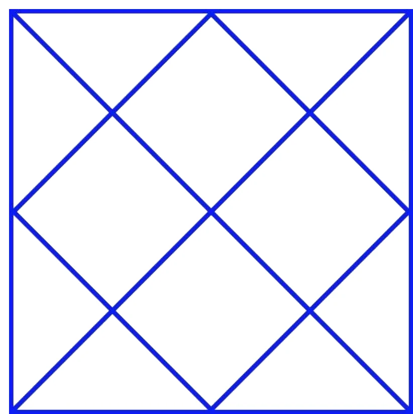
Full question on page 3 of the official paper (PDF)
Show answerHide answer
Key idea: Apart from the outer square, every rectangle is tilted: its sides lie on the three lines of each diagonal direction.
Official answer: C
Inside the square there are three parallel lines in each diagonal direction: the diagonal itself and the two sides of the inner tilted square. A tilted rectangle needs two lines from each direction, and every such choice has all four corners inside the outer square:
\binom{3}{2} \times \binom{3}{2} = 9These are the four small squares, the four rectangles made of two small squares, and the inner tilted square. With the outer square, 9 + 1 = 10. Option (C).
Learn the idea:
Q.6
General Aptitude2 marksMCQ
Forestland is a planet inhabited by different kinds of creatures. Among other creatures, it is populated by animals all of whom are ferocious. There are also creatures that have claws, and some that do not. All creatures that have claws are ferocious. Based only on this information, which option can be logically inferred with certainty?
Full question on page 4 of the official paper (PDF)
Show answerHide answer
Key idea: Clawed creatures exist and all of them are ferocious, so the two sets overlap.
Official answer: D
Creatures with claws exist, and every one of them is ferocious, so at least some ferocious creatures have claws: (D) follows.
(B) and (C) contradict "all creatures that have claws are ferocious", and (A) isn't stated: a clawed creature could be ferocious without being an animal. Option (D).
Q.7
General Aptitude2 marksMCQ
Which one of the following options represents the graph in the figure?
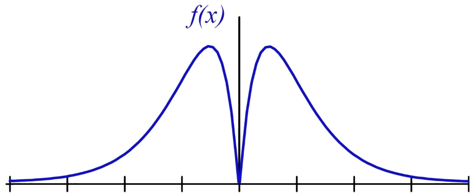
Full question on page 5 of the official paper (PDF)
Show answerHide answer
Key idea: The graph is symmetric about the y-axis and never negative, so f must be even and non-negative.
Official answer: A
Test each option for an even, non-negative function:
- (A) x^2 2^{-|x|}: even, zero at 0, positive elsewhere, and decays as |x| grows. It matches.
- (B) x\, 2^{-|x|} is odd: negative for x < 0.
- (C) |x|\, 2^{-x} grows without bound as x \to -\infty.
- (D) x\, 2^{-x} is negative for x < 0 and grows in size as x \to -\infty.
Option (A). Its peaks are where 2x - x^2 \ln 2 = 0, at x = \pm 2/\ln 2 \approx \pm 2.885.
Learn the idea:
Q.8
General Aptitude2 marksMCQ
Which one of the following options can be inferred from the passage alone? "When I was a kid, I was partial to stories about other worlds and interplanetary travel. I used to imagine that I could just gaze off into space and be whisked to another planet." [Excerpt from The Truth about Stories by T. King]
Full question on page 6 of the official paper (PDF)
Show answerHide answer
Key idea: "When I was a kid" and the past tense mean the speaker is no longer a child.
Official answer: B
The narrator looks back ("When I was a kid", "I used to imagine"), so this is an adult remembering a childhood liking. Option (B).
(A) needs the speaker to be a child now. Partial to means fond of, not reading in parts, so (C) misreads it, and the passage draws no lesson, so (D) goes beyond it.
Q.9
General Aptitude2 marksMCQ
Out of 1000 individuals in a town, 100 unidentified individuals are covid positive. To identify them with few testing kits, the authorities (i) collect saliva samples from all 1000 and randomly group them into sets of 5, (ii) mix the samples in each set and test the mixed sample, (iii) if that test is negative, declare all 5 negative, and (iv) if it is positive, test all 5 separately. With this strategy, no more than ____ testing kits will be required to identify all 100 positives, however they are grouped.
Full question on page 7 of the official paper (PDF)
Show answerHide answer
Key idea: The worst case puts every positive in a different group, so as many groups as possible need five more tests.
Official answer: A
There are 1000 / 5 = 200 groups, so 200 kits test the mixed samples. Each positive group then needs 5 more kits. The most positive groups there can be is 100, one positive in each:
200 + 100 \times 5 = 700Option (A).
Q.10
General Aptitude2 marksMCQ
A 100 cm × 32 cm rectangular sheet is folded 5 times. Each time, the long edge aligns with its opposite side. In the end, the folded sheet is a rectangle of 100 cm × 1 cm. How many creases are visible when the sheet is unfolded?
Full question on page 8 of the official paper (PDF)
Show answerHide answer
Key idea: Each fold halves the 32 cm side, and in the end the creases split it into 1 cm strips.
Official answer: C
Five halvings take the 32 cm side to 32 / 2^5 = 1 cm. Unfolded, the sheet is divided into 32 strips of 1 cm, and 32 strips have 31 creases between them. Fold by fold, the creases add up as 1 + 2 + 4 + 8 + 16 = 31. Option (C).
Q.11
Engineering Mathematics1 markMCQ
Let and . What value of the coefficient in minimises the length of the error vector ?
Full question on page 9 of the official paper (PDF)
Show answerHide answer
Key idea: The error is shortest when it is perpendicular to \mathbf{v}_2, which makes \alpha \mathbf{v}_2 the projection of \mathbf{v}_1.
Official answer: C
Setting \mathbf{e} \cdot \mathbf{v}_2 = 0 gives the projection coefficient:
Option (C).
Learn the idea:
Q.12
Engineering Mathematics1 markMCQ
What is the rate of increase of the scalar field in the direction at the point ?
Full question on page 9 of the official paper (PDF)
Show answerHide answer
Key idea: The rate of increase along a direction is the gradient dotted with the unit vector in that direction.
Official answer: B
Option (B). Forgetting to normalise \mathbf{v} gives 4, option (D).
Learn the idea:
Q.13
Engineering Mathematics1 markMCQ
Let . Which of the following cannot be a value of ?
Full question on page 10 of the official paper (PDF)
Show answerHide answer
Key idea: Write 16j in polar form; its four fourth roots have modulus 2 and angles a quarter turn apart.
Official answer: A
The angles are \pi/8, 5\pi/8, 9\pi/8 and 13\pi/8. 2\pi/8 is not among them: (2e^{j\pi/4})^4 = 16e^{j\pi} = -16. Option (A).
Learn the idea:
Q.14
Engineering Mathematics1 markMCQ
What is the value of the contour integral , where is the circle , taken counter-clockwise?
Full question on page 10 of the official paper (PDF)
Show answerHide answer
Key idea: Find which poles lie inside the circle, then use the residue theorem.
Official answer: B
The poles are the roots of z^2 + 2z + 2, z = -1 \pm j. The circle has centre -1 + 1.5j and radius 1, so -1 + j (distance 0.5) is inside and -1 - j (distance 2.5) is not.
Option (B).
Learn the idea:
Q.15
Engineering Mathematics1 markMCQ
The eigenvalues and eigenvectors of a matrix are and . For any invertible matrix , what are the eigenvalues and eigenvectors of the matrix , where ?
Full question on page 11 of the official paper (PDF)
Show answerHide answer
Key idea: Similar matrices share eigenvalues; multiply B\mathbf{v}_k = \lambda_k \mathbf{v}_k by P to see the eigenvectors.
Official answer: C
So A has the same eigenvalues \lambda_k, with eigenvectors P\mathbf{v}_k. Option (C).
Learn the idea:
Q.16
Electronic Devices1 markMCQ
In a semiconductor, if the Fermi energy level lies in the conduction band, the semiconductor is known as
Full question on page 11 of the official paper (PDF)
Show answerHide answer
Key idea: A Fermi level near the conduction band means n-type; one inside a band means degenerate doping.
Official answer: A
Doping with donors pushes E_F up towards E_C. Very heavy donor doping pushes it past E_C into the conduction band, where Boltzmann statistics no longer hold: the semiconductor is degenerate. Option (A).
A degenerate p-type semiconductor has E_F inside the valence band instead.
Learn the idea:
Q.17
Electronic Devices1 markMCQ
For an intrinsic semiconductor at temperature K, which of the following statements is true?
Full question on page 12 of the official paper (PDF)
Show answerHide answer
Key idea: At 0 K no electron has the thermal energy to cross the band gap.
Official answer: A
At 0 K the Fermi function is a step at E_F, which lies in the gap: every state below it is full and every state above it is empty. So the valence band is full and the conduction band is empty, which is why an intrinsic semiconductor is an insulator at 0 K. Option (A).
Q.18
Networks, Signals and Systems1 markMCQ
A series circuit has a quality factor of 1000 at a centre frequency of rad/s. What are possible values of , and ?
Full question on page 12 of the official paper (PDF)
Show answerHide answer
Key idea: For a series RLC, \omega_0 = 1/\sqrt{LC} and Q = \omega_0 L / R.
Official answer: D
Every option has L = 1\ \muH and C = 1\ \muF, so \omega_0 = 1/\sqrt{10^{-12}} = 10^6 rad/s, as required. Then
Option (D).
Learn the idea:
Q.19
Electronic Devices1 markMCQ
For a MOS capacitor, and are the flat-band and threshold voltages. Which graph in the figure best represents the depletion width as the gate voltage varies?
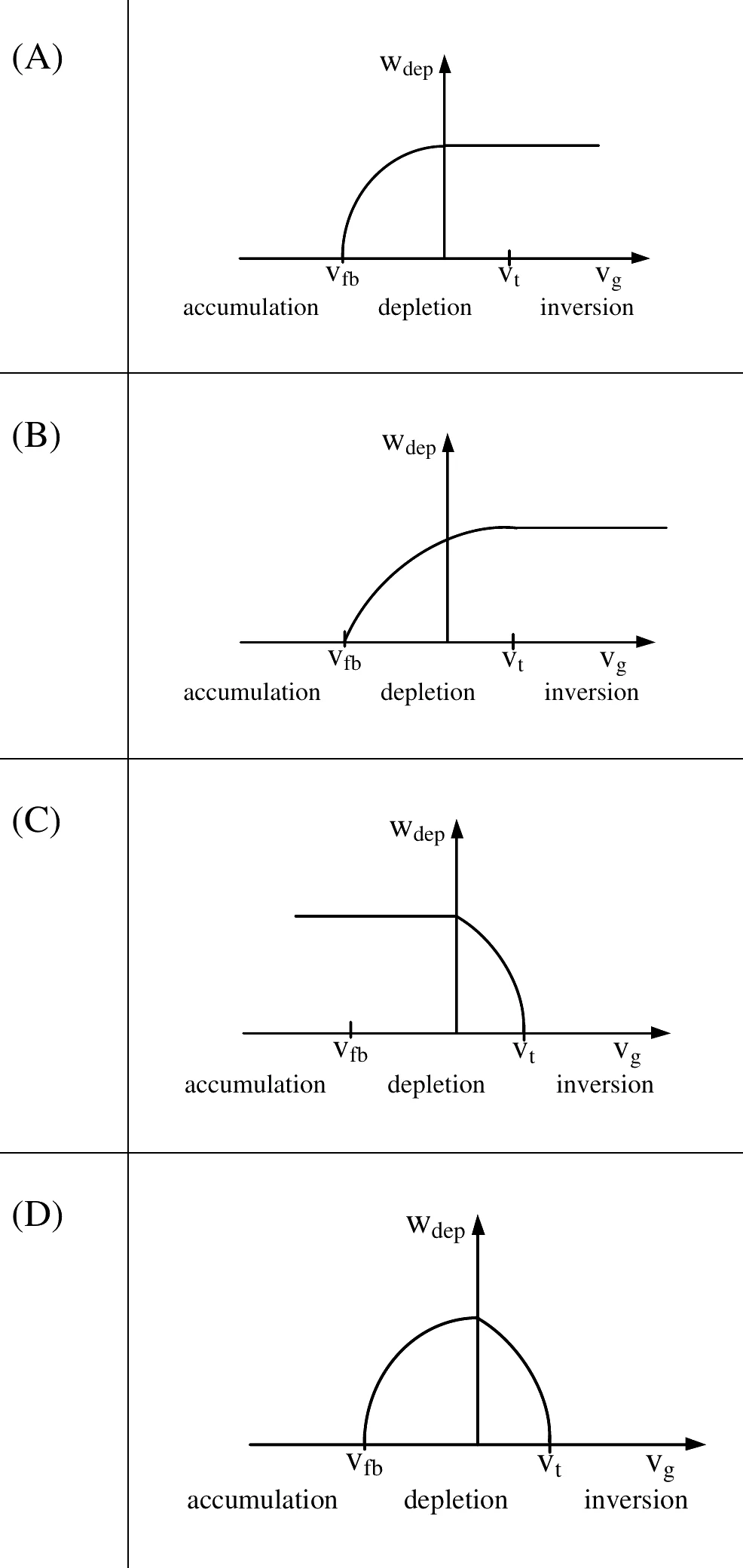
Full question on page 13 of the official paper (PDF)
Show answerHide answer
Key idea: There is no depletion layer in accumulation; it grows through depletion and stops growing once the inversion layer forms.
Official answer: B
Below V_{fb} (accumulation) majority carriers pile up at the surface and W_{dep} = 0. Between V_{fb} and V_t the depletion layer widens as V_g rises. At V_t the inversion layer forms and screens any further charge, so W_{dep} stays at its maximum, W_{max}, through inversion.
Graph (B) shows exactly this: zero, a smooth rise through depletion, and a flat line beyond V_t. (A) saturates before V_t, and (C) and (D) fall to zero at V_t. Option (B).
Q.20
Electromagnetics1 markMCQ
A narrow-band signal propagates in a lossless dielectric medium (, ) with phase velocity and group velocity . Which statement is true? ( is the velocity of light in vacuum.)
Full question on page 14 of the official paper (PDF)
Show answerHide answer
Key idea: A lossless dielectric with constant \varepsilon_r is not dispersive, so v_g = v_p.
Official answer: D
v_p = \frac{\omega}{\beta} = \frac{c}{\sqrt{\mu_r \varepsilon_r}} = \frac{c}{2}\beta = \omega\sqrt{\mu\varepsilon} is proportional to \omega, so v_g = d\omega/d\beta is also c/2. Both are less than c. Option (D).
Q.21
Analog Circuits1 markMCQ
In the circuit in the figure, and are bias voltages. Based on its input and output impedances, the circuit behaves as a
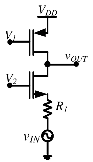
Full question on page 15 of the official paper (PDF)
Show answerHide answer
Key idea: Low input impedance means the input is a current; high output impedance means the output is a current.
Official answer: D
The NMOS is a common-gate stage: its gate is held at V_2 and the signal enters at its source. Looking into a source the impedance is about 1/g_m, which is low, so the stage takes a current as its input.
The output is taken at the drains, where the NMOS drain and the PMOS current source (gate at V_1) both look like high impedances, about r_o each, so the output behaves as a current. Low input impedance and high output impedance make a current controlled current source, a current buffer. Option (D).
Q.22
Analog Circuits1 markMCQ
A cascade of common-source amplifiers in a unity gain feedback configuration oscillates when
Full question on page 15 of the official paper (PDF)
Show answerHide answer
Key idea: A question given marks to all scores full marks for every candidate, whatever they answered.
Official answer: Marks to all
The key awards marks to all for this question and doesn't say why, so we don't pick an option.
The idea behind it: a feedback amplifier oscillates when the loop gain reaches 1 in magnitude at the frequency where the loop's phase shift makes the feedback positive (the Barkhausen condition). One likely reason for the ruling is that the options state the condition in terms of the closed-loop gain and a strict inequality on the phase, so none of them states the condition exactly.
Ruling in the key: The key gives marks to all (MTA) for this question: every candidate received its 1 mark.
Q.23
Digital Circuits1 markMCQ
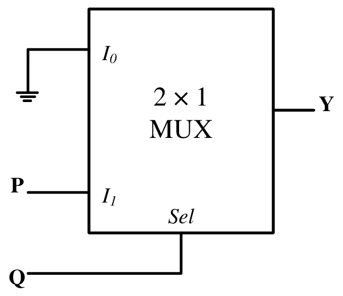
In the circuit in the figure, P and Q are the inputs of a 2 × 1 multiplexer: is grounded, and the select line is Q. What logical function does it realise?
Full question on page 16 of the official paper (PDF)
Show answerHide answer
Key idea: A 2 × 1 multiplexer gives Y = \bar{S} I_0 + S I_1.
Official answer: A
Y = \bar{Q} \cdot 0 + Q \cdot P = PQY is 1 only when Q selects I_1 and P is 1: an AND gate. Option (A).
Learn the idea:
Q.24
Digital Circuits1 markMCQ
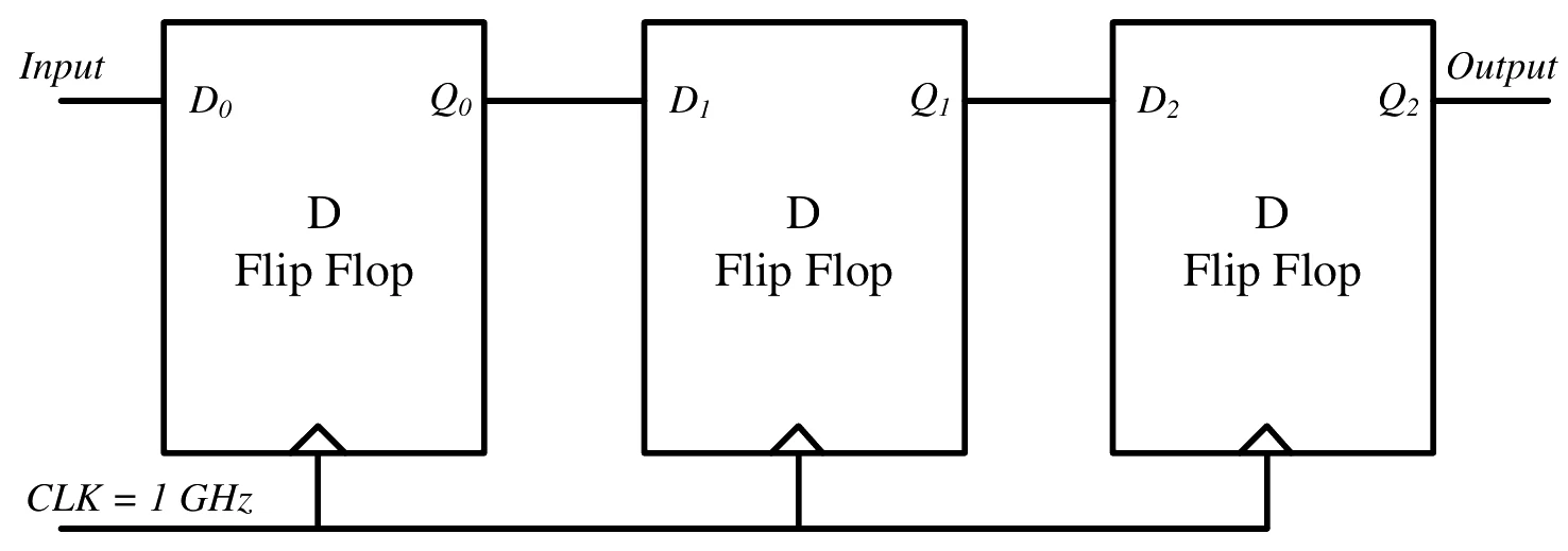
The synchronous sequential circuit in the figure, three D flip-flops in a chain sharing one clock, works at a clock frequency of 1 GHz. What are its throughput, in Mbits/s, and its latency, in ns?
Full question on page 17 of the official paper (PDF)
Show answerHide answer
Key idea: A new bit enters on every clock edge, and each bit needs one clock per flip-flop to reach the output.
Official answer: A
Like a pipeline, the chain accepts one new bit every clock period of 1 ns, so its throughput is one bit per ns, 1000 Mbit/s.
Each bit moves one flip-flop per clock, so it appears at Q_2 three clocks after it enters: a latency of 3 ns. Option (A).
Learn the idea:
Q.25
Control Systems1 markMCQ
The open-loop transfer function of a unity negative feedback system is , where , and are positive constants. What is the phase crossover frequency, in rad/s?
Full question on page 18 of the official paper (PDF)
Show answerHide answer
Key idea: At the phase crossover frequency the phase of G(j\omega) is -180°.
Official answer: A
So \tan^{-1}(\omega T_1) + \tan^{-1}(\omega T_2) = 90°, which needs \omega T_1 \cdot \omega T_2 = 1:
\omega_{pc} = \frac{1}{\sqrt{T_1 T_2}}Option (A).
Q.26
Networks, Signals and Systems1 markMCQ
A system has input and output . The system is
Full question on page 18 of the official paper (PDF)
Show answerHide answer
Key idea: Causal means y(t) uses no input later than t; time invariant means a delayed input gives the same output, delayed.
Official answer: B
Causality: e^t > t for every t, so y(t) always uses the input at a later time. At t = 0, y(0) = x(1). The system is non-causal.
Time invariance: delaying the input by t_0 gives x(e^t - t_0), but delaying the output gives y(t - t_0) = x(e^{t - t_0}). These differ, so the system is time varying. Option (B).
Q.27
Communications1 markMCQ
Let be a strictly band-limited signal with bandwidth and energy . Assuming , what is the energy in the signal ?
Full question on page 19 of the official paper (PDF)
Show answerHide answer
Key idea: Modulation splits the spectrum into two half-height copies; with \omega_0 > B they don't overlap.
Official answer: B
The Fourier transform of m(t)\cos\omega_0 t is
\tfrac{1}{2}\left[M(\omega - \omega_0) + M(\omega + \omega_0)\right]Each copy has a quarter of the energy density, |M|^2/4, and since \omega_0 = 10B the copies don't overlap, so the energies add: E/4 + E/4 = E/2. Option (B). In the time domain, \cos^2\omega_0 t = \tfrac{1}{2}(1 + \cos 2\omega_0 t), and the \cos 2\omega_0 t part integrates to zero.
Learn the idea:
Q.28
Networks, Signals and Systems1 markMCQ
What is the Fourier transform of ? (Note: .)
Full question on page 19 of the official paper (PDF)
Show answerHide answer
Key idea: Complete the square in the exponent, then use the given integral.
Official answer: C
A quick check: X(0) must equal \int x(t)\, dt = \sqrt{\pi}, which rules out (B), and (A) grows with \omega. Option (C).
Q.29
Networks, Signals and Systems1 markMCQ
Match each signal type with its spectral characteristics. Signal types: (i) continuous, aperiodic; (ii) continuous, periodic; (iii) discrete, aperiodic; (iv) discrete, periodic. Spectral characteristics: (a) continuous, aperiodic; (b) continuous, periodic; (c) discrete, aperiodic; (d) discrete, periodic.
Full question on page 20 of the official paper (PDF)
Show answerHide answer
Key idea: Periodic in one domain means discrete in the other, and discrete in one domain means periodic in the other.
Official answer: B
- (i) Continuous, aperiodic: the Fourier transform, continuous and aperiodic, (a).
- (ii) Continuous, periodic: the Fourier series, discrete lines, aperiodic, (c).
- (iii) Discrete, aperiodic: the DTFT, continuous and periodic in 2\pi, (b).
- (iv) Discrete, periodic: the DFS, discrete and periodic, (d).
Option (B).
Learn the idea:
Q.30
Communications1 markMSQ
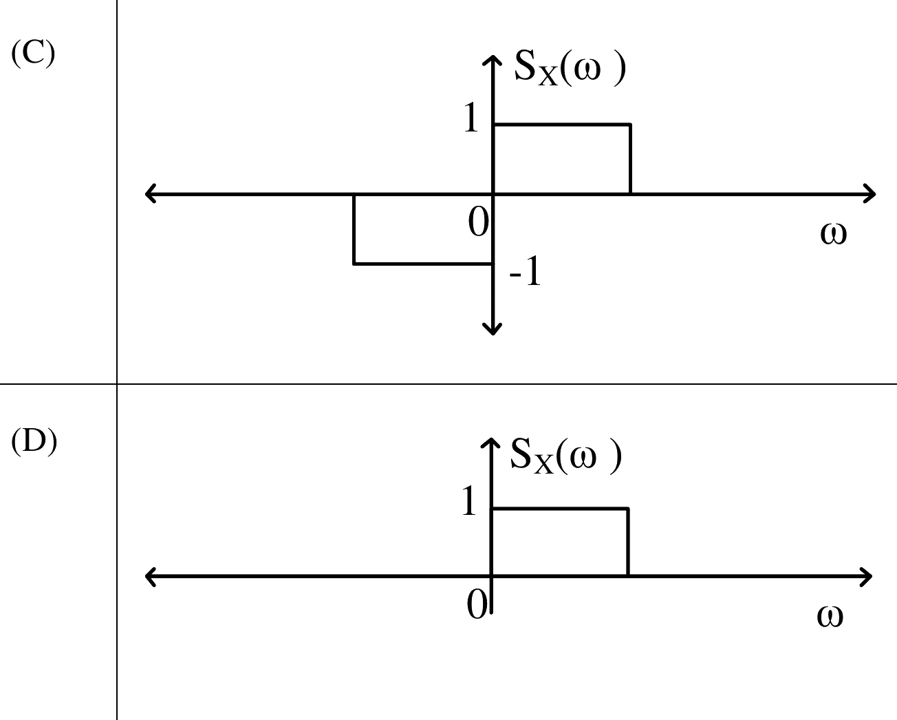
For a real signal, which of the following is/are valid power spectral density/densities? Options (C) and (D) are the plots in the figure.
One or more options are correct.
Full question on page 21 of the official paper (PDF)
Show answerHide answer
Key idea: The PSD of a real signal is real, never negative, and even in \omega.
Official answer: A and B
- (A) 2/(9 + \omega^2) is positive and even: valid. It is the PSD of e^{-3|\tau|}/3.
- (B) e^{-\omega^2}\cos^2\omega is never negative and is even: valid.
- (C) is negative for \omega < 0: not a PSD.
- (D) is not even: for a real signal S_X(-\omega) = S_X(\omega), so a one-sided band isn't valid.
Options (A) and (B).
Q.31
Digital Circuits1 markNAT
The signal-to-noise ratio (SNR) of an ADC with a full-scale sinusoidal input is 61.96 dB. What is the resolution of the ADC, in bits?
Answer format: bits, rounded off to the nearest integer
Full question on page 21 of the official paper (PDF)
Show answerHide answer
Key idea: For an ideal N-bit ADC and a full-scale sine, \text{SNR} = 6.02N + 1.76 dB.
Official answer: 10
The formula comes from a full-scale sine's power, (2^N \Delta)^2/8, over the quantisation noise power, \Delta^2/12: their ratio is 1.5 \times 4^N, which is 1.76 + 6.02N dB. Answer: 10 bits.
Learn the idea:
Q.32
Networks, Signals and Systems1 markNAT
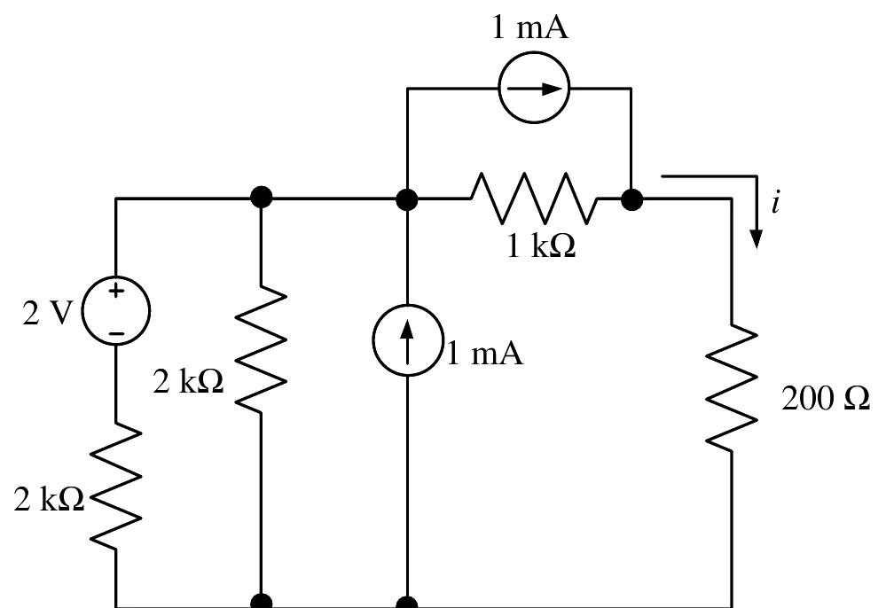
In the circuit in the figure, what is the current flowing through the 200 Ω resistor, in mA?
Answer format: mA, rounded off to two decimal places
Full question on page 22 of the official paper (PDF)
Show answerHide answer
Key idea: Two unknown node voltages: write KCL at each, working in volts, mA and kΩ.
Official answer: 1.30 to 1.40
Call the top-left node A and the node above the 200 Ω resistor B. In mA and kΩ, KCL at A (the 1 mA into A from below and the 1 mA out of A to B cancel):
KCL at B, with the 1 mA source feeding it:
So V_A = (1 + V_B)/2, and 5.5\,V_B = 1.5 gives V_B = 0.2727 V. Then i = V_B / 0.2\ \text{k}\Omega = 1.36 mA.
Learn the idea:
Q.33
Networks, Signals and Systems1 markNAT
For the two-port network in the figure, S. It is driven by a 120 V source through 10 Ω at port 1. What load impedance , in Ω, takes the maximum power?
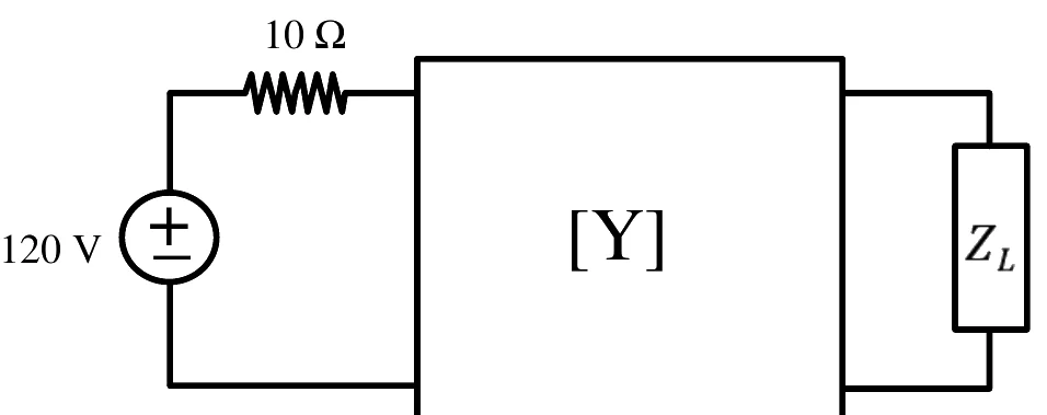
Answer format: Ohms, rounded off to the nearest integer
Full question on page 22 of the official paper (PDF)
Show answerHide answer
Key idea: Maximum power needs Z_L equal to the Thevenin impedance seen at port 2, with the source shorted.
Official answer: 80
With the source shorted, port 1 sees I_1 = -V_1/10, so -0.1V_1 = 0.02V_1 - 0.01V_2, which gives V_1 = V_2/12. Then
So Z_{th} = 1/0.0125 = 80 Ω, and Z_L = 80 Ω. Equivalently, Y_{out} = Y_{22} - Y_{12}Y_{21}/(Y_{11} + 0.1). Answer: 80.
Learn the idea:
Q.34
Digital Circuits1 markNAT
For the circuit in the figure, two cross-coupled NAND gates with inputs A and B and outputs Q and , the propagation delay of each NAND gate is 1 ns. What is the critical path delay, in ns?
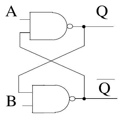
Answer format: ns, rounded off to the nearest integer
Full question on page 23 of the official paper (PDF)
Show answerHide answer
Key idea: A change only settles once it has gone through one gate and been fed back through the other.
Official answer: 2
Pull A low to set the latch: after 1 ns the first gate's output Q goes high. Only then does the second gate see the new Q, and after another 1 ns \overline{Q} goes low and holds Q. The outputs are settled after two gate delays, so the critical path is 2 ns.
Learn the idea:
Q.35
Networks, Signals and Systems1 markNAT
In the circuit in the figure, a 2 V source drives, through switch S and 1 Ω, a 2 Ω resistor in parallel with a 1 H inductor. S was closed for a long time and is opened at . What is the maximum magnitude of the voltage across the 2 Ω resistor, in volts?
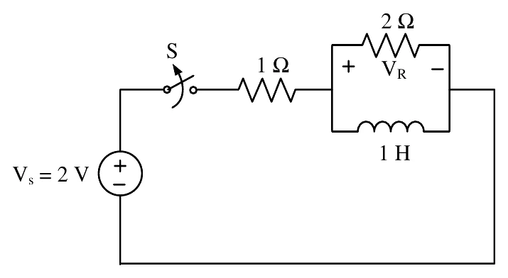
Answer format: volts, rounded off to the nearest integer
Full question on page 23 of the official paper (PDF)
Show answerHide answer
Key idea: The inductor current can't change instantly, and once S opens it has nowhere to go but the 2 Ω resistor.
Official answer: 4
Before t = 0 the inductor is a short, so V_R = 0 and the whole current, 2/1 = 2 A, flows through the inductor.
After S opens, the inductor and the 2 Ω resistor form a loop, and the 2 A must flow through the resistor: |V_R(0^+)| = 2 \times 2 = 4 V. It then decays as 4e^{-2t}, so the maximum magnitude is 4 V.
Q.36
Engineering Mathematics2 marksMCQ
A random variable , distributed normally as , undergoes the transformation in the figure. What is the form of the probability density function of ? (In the options, , , are non-zero constants and is a piecewise continuous function.)
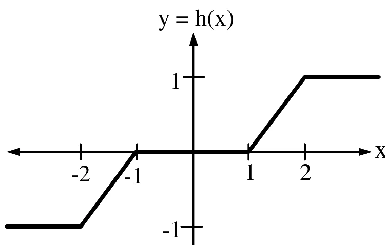
Full question on page 24 of the official paper (PDF)
Show answerHide answer
Key idea: Wherever h is flat over an interval of x, all that probability lands on one value of y: an impulse in the PDF.
Official answer: B
h is flat at three levels: y = -1 for x < -2, y = 0 for -1 < x < 1 and y = 1 for x > 2. Each of these ranges has non-zero probability under N(0, 1), so the PDF has impulses at y = -1, 0 and 1:
The sloped parts map 1 < |x| < 2 continuously onto 0 < |y| < 1, which gives g(y). Option (B).
Learn the idea:
Q.37
Engineering Mathematics2 marksMCQ
What is the value of the line integral along the straight line joining and ?
Full question on page 25 of the official paper (PDF)
Show answerHide answer
Key idea: The integrand is an exact differential, so the integral depends only on the end points.
Official answer: B
Option (B). Parametrising the line as (1 + t, 1 + 2t, 2 - t) gives the same 24.
Learn the idea:
Q.38
Engineering Mathematics2 marksMCQ
Let be an real column vector with length . What is the trace of the matrix ?
Full question on page 25 of the official paper (PDF)
Show answerHide answer
Key idea: The diagonal of \mathbf{x}\mathbf{x}^T holds the squares x_i^2.
Official answer: A
Option (A).
Learn the idea:
Q.39
Analog Circuits2 marksMCQ
In the circuit in the figure, drives an inverting amplifier (, ) and a non-inverting amplifier (, ); their outputs feed, each through , the inverting input of a third op-amp with feedback and its non-inverting input grounded. What is ?
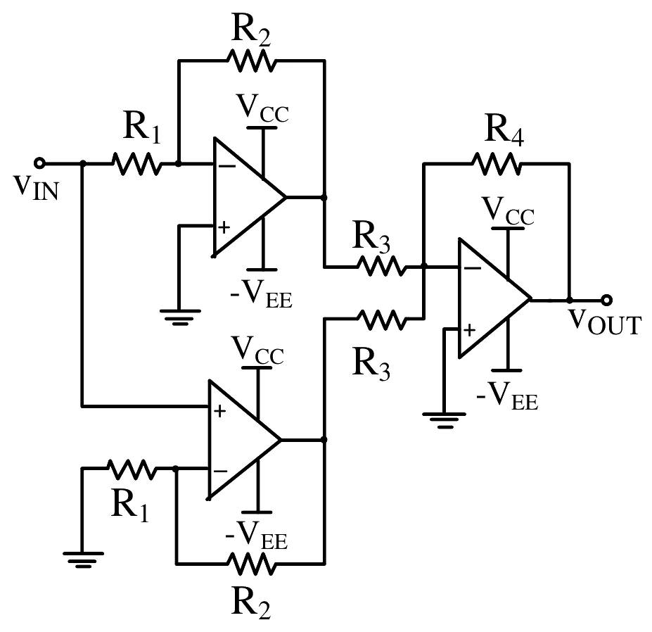
Full question on page 26 of the official paper (PDF)
Show answerHide answer
Key idea: The third op-amp is an inverting summer, and the first two outputs add to exactly v_{IN}.
Official answer: A
The summer gives v_{OUT} = -\dfrac{R_4}{R_3}(v_1 + v_2) = -\dfrac{R_4}{R_3} v_{IN}. Option (A).
Learn the idea:
Q.40
Analog Circuits2 marksMCQ
In the circuit in the figure, and are silicon diodes with a cut-in voltage of 0.7 V, connected in anti-parallel between and ; connects through 1 kΩ to a 1 V source. Which transfer characteristic is correct?
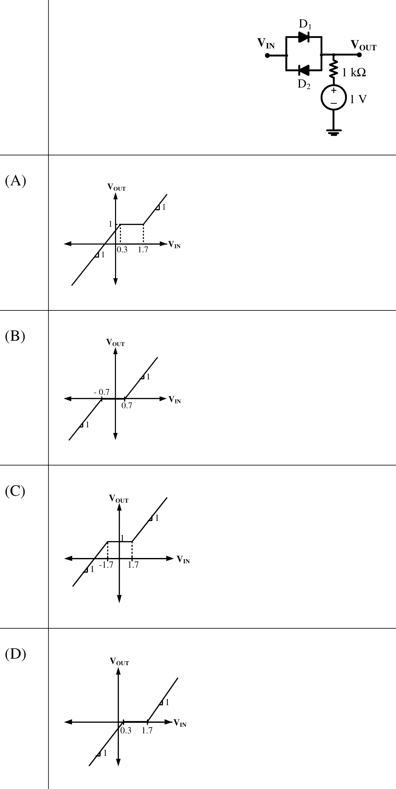
Full question on page 27 of the official paper (PDF)
Show answerHide answer
Key idea: With no diode on, no current flows in the 1 kΩ, so V_{OUT} sits at 1 V.
Official answer: A
While |V_{IN} - 1| < 0.7, neither diode conducts, no current flows and V_{OUT} = 1 V: that is 0.3 \le V_{IN} \le 1.7.
For V_{IN} > 1.7, D_1 conducts and V_{OUT} = V_{IN} - 0.7. For V_{IN} < 0.3, D_2 conducts and V_{OUT} = V_{IN} + 0.7. Both have slope 1, joining the flat part at 1 V. Option (A).
Learn the idea:
Q.41
Control Systems2 marksMCQ
The closed-loop system in the figure has unity negative feedback round , where and . What is the steady-state error due to a ramp input, ?
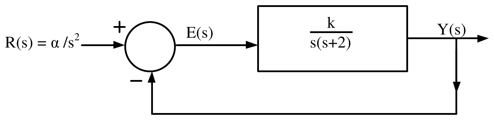
Full question on page 28 of the official paper (PDF)
Show answerHide answer
Key idea: A type-1 loop follows a ramp with a constant error, \alpha / K_v, where K_v = \lim_{s \to 0} sG(s).
Official answer: A
This holds when the loop is stable, which it is for every k > 0: the characteristic equation s^2 + 2s + k = 0 has both roots in the left half-plane. Option (A).
Q.42
Control Systems2 marksMCQ
In the block diagram in the figure, and are two inputs, and the output is . What are and ?
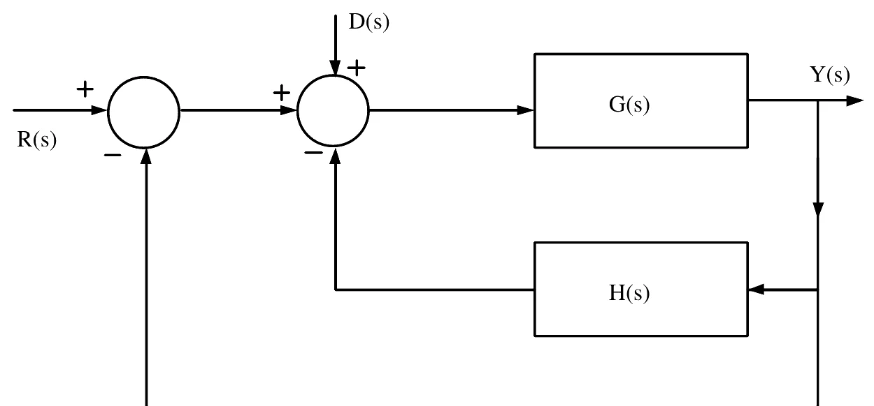
Full question on page 29 of the official paper (PDF)
Show answerHide answer
Key idea: Write the signal into G and solve once for Y; both inputs enter at the same point, so they share a denominator.
Official answer: A
The second junction adds D to the first junction's output, R - Y, and subtracts HY:
Y = G\left[(R - Y) + D - HY\right]Collecting the Y terms:
Y(1 + G + GH) = G R + G DSo G_1 = G_2 = G/(1 + G + GH). Option (A).
Q.43
Control Systems2 marksMCQ
The state equation of a second-order system is , with initial condition . and are two distinct eigenvalues of , and and the corresponding eigenvectors. For constants and , what is the solution ?
Full question on page 30 of the official paper (PDF)
Show answerHide answer
Key idea: Try \mathbf{x} = e^{\lambda t}\mathbf{v}: it solves the equation exactly when A\mathbf{v} = \lambda\mathbf{v}.
Official answer: A
Distinct eigenvalues give independent eigenvectors, so every solution is \alpha_1 e^{\lambda_1 t}\mathbf{v}_1 + \alpha_2 e^{\lambda_2 t}\mathbf{v}_2, with \alpha_1, \alpha_2 fixed by \mathbf{x}(0). In (B) to (D), \dot{\mathbf{x}} would be k\lambda_i times each term, not A\mathbf{x}. Option (A).
Learn the idea:
Q.44
Networks, Signals and Systems2 marksMCQ
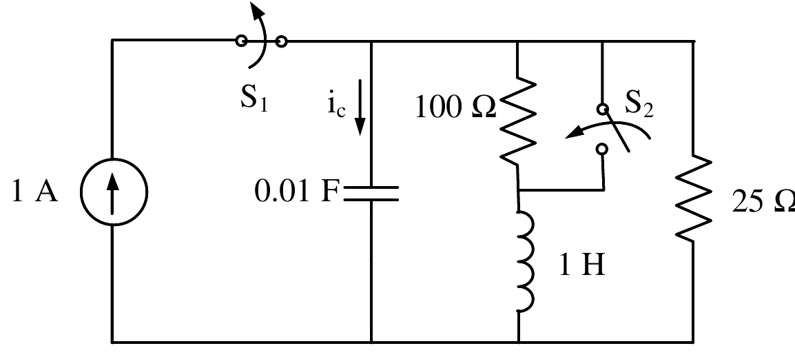
In the circuit in the figure, switch was closed and was open for a long time. At , is opened and is closed, simultaneously. shorts the 100 Ω resistor that is in series with the 1 H inductor. What is , in amperes?
Full question on page 31 of the official paper (PDF)
Show answerHide answer
Key idea: Find the capacitor voltage and inductor current before switching; both carry over to t = 0^+.
Official answer: B
Before t = 0 the capacitor is open and the inductor a short, so the 1 A splits between the 100 Ω branch and the 25 Ω resistor:
At t = 0^+ the source is gone, v_C = 20 V and i_L = 0.2 A. With the 100 Ω shorted, the inductor still carries 0.2 A, and the 25 Ω carries 20/25 = 0.8 A. The capacitor supplies both, so the current down into it is i_C(0^+) = -(0.2 + 0.8) = -1 A. Option (B).
Learn the idea:
Q.45
Communications2 marksMCQ
An FM signal , where has bandwidth , is passed through a non-linear system with output . Let denote the FM bandwidth. What is the minimum value of required to recover from ?
Full question on page 32 of the official paper (PDF)
Show answerHide answer
Key idea: Squaring an FM wave gives a DC term and an FM wave at 2\omega_c with twice the deviation, so twice the bandwidth.
Official answer: B
The term at 2\omega_c occupies 2\omega_c \pm B_T (twice the deviation, so twice the bandwidth), while x(t) occupies \omega_c \pm B_T/2, and the DC term sits at 0. A bandpass filter can keep x(t) alone if the bands don't overlap:
The DC term needs only \omega_c > B_T/2, which this already meets. Option (B).
Q.46
Networks, Signals and Systems2 marksMCQ
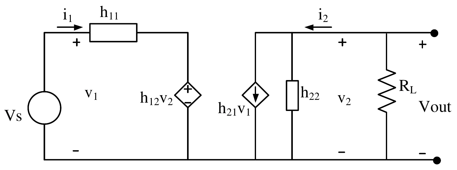
The h-parameter model of a two-port network is shown in the figure, driven by and loaded by . What is the condition for the maximum small-signal voltage gain ?
Full question on page 33 of the official paper (PDF)
Show answerHide answer
Key idea: A question given marks to all scores full marks for every candidate, whatever they answered.
Official answer: Marks to all
The key awards marks to all for this question and doesn't say why, so we don't pick an option.
The idea behind it: with V_s driving port 1 directly, the gain of an h-parameter two-port is -h_{21}R_L / \left(h_{11} + \Delta h\, R_L\right) with \Delta h = h_{11}h_{22} - h_{12}h_{21}, so a large h_{21} and small h_{11}, h_{12} and h_{22} raise it. One likely reason for the ruling is the figure: it labels the output source h_{21}v_1 where the h-parameter model has h_{21}i_1, and with h_{11} = 0 and h_{12} = 0 the input current isn't set by V_s at all.
Ruling in the key: The key gives marks to all (MTA) for this question: every candidate received its 2 marks.
Q.47
Networks, Signals and Systems2 marksMCQ
A discrete-time periodic signal has period and DTFS , with , , , and . What is ?
Full question on page 34 of the official paper (PDF)
Show answerHide answer
Key idea: \sum_n x[n] e^{-jk2\pi n/N} = N a_k, so write the sine as two exponentials.
Official answer: A
\sin\frac{4\pi n}{5} = \frac{e^{j4\pi n/5} - e^{-j4\pi n/5}}{2j}\sum_n x[n] e^{-j2(2\pi n/5)} = 5a_2 = 10j, and \sum_n x[n] e^{+j2(2\pi n/5)} = 5a_{-2} = 5a_3 = -10j. So
Option (A).
Learn the idea:
Q.48
Networks, Signals and Systems2 marksMCQ
An input with DTFT is passed through an LTI system with frequency response . What is the output ?
Full question on page 34 of the official paper (PDF)
Show answerHide answer
Key idea: Multiply the two polynomials in e^{-j\Omega}; each power e^{-jk\Omega} is a \delta[n-k].
Official answer: C
The e^{-j3\Omega} term collects 2 from X and +\tfrac{1}{2} from (-e^{-j\Omega})(-\tfrac{1}{2}e^{-j2\Omega}). So y[n] = \delta[n] - \delta[n-1] - \tfrac{1}{2}\delta[n-2] + \tfrac{5}{2}\delta[n-3] - \delta[n-5]. Option (C).
Learn the idea:
Q.49
Networks, Signals and Systems2 marksMCQ
is passed through an LTI system with impulse response . What is the output?
Full question on page 35 of the official paper (PDF)
Show answerHide answer
Key idea: \sin Wt/(\pi t) is an ideal low-pass of height 1 and cut-off W; squaring it makes a triangle in frequency.
Official answer: A
\dfrac{\sin Wt}{\pi t} transforms to a rectangle of height 1 on |\omega| < W. Its square transforms to \tfrac{1}{2\pi} times the rectangle convolved with itself: a triangle of peak \tfrac{2W}{2\pi} = \tfrac{W}{\pi}, reaching zero at |\omega| = 2W. Times \pi, the peak is W:
Multiplying by \cos 10Wt shifts half of it to each of \pm 10W: H(\omega) = \tfrac{1}{2}[T(\omega - 10W) + T(\omega + 10W)]. At \omega = 10.5W, 0.5W from the centre:
H is real and positive, so there is no phase shift: y(t) = 10 \cdot \tfrac{3W}{8}\cos(10.5Wt) = \tfrac{15W}{4}\cos(10.5Wt). Option (A).
Q.50
Networks, Signals and Systems2 marksMCQ
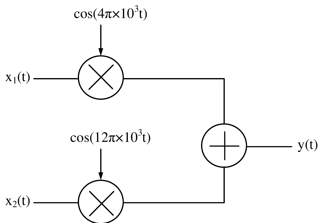
and are band-limited signals, each with bandwidth rad/s. In the figure, . What Nyquist sampling frequency, in rad/s, is required to sample ?
Full question on page 36 of the official paper (PDF)
Show answerHide answer
Key idea: Find the highest frequency in y(t) and double it.
Official answer: D
Multiplying by a cosine shifts the spectrum to the carrier. x_1 reaches 4\pi + 4\pi = 8\pi \times 10^3 rad/s, and x_2 reaches 12\pi + 4\pi = 16\pi \times 10^3 rad/s. The highest frequency is 16\pi \times 10^3, so
Option (D).
Learn the idea:
Q.51
Electromagnetics2 marksMCQ
The S-parameters of a two-port network are , with reference to . Two lossless transmission line sections of electrical lengths and are added to the input and output ports, respectively. What are the S-parameters of the resulting two-port?
Full question on page 37 of the official paper (PDF)
Show answerHide answer
Key idea: Each pass along a lossless line delays a wave by its electrical length, a factor e^{-j\theta}.
Official answer: A
A wave reflected at port 1 crosses the input line twice, in and back out: S'_{11} = S_{11}e^{-j2\theta_1}. Likewise S'_{22} = S_{22}e^{-j2\theta_2}.
A wave passing through crosses both lines once each: S'_{21} = S_{21}e^{-j(\theta_1 + \theta_2)}, and the same for S'_{12}. Every factor is a delay, so every exponent is negative. Option (A).
Learn the idea:
Q.52
Electromagnetics2 marksMSQ
The standing wave ratio on a 50 Ω lossless line terminated in an unknown load is 2.0. Successive voltage minima are 30 cm apart, and the first minimum is 10 cm from the load. can be replaced by an equivalent length of the same line terminated in a resistance . What are and ?
One or more options are correct.
Full question on page 38 of the official paper (PDF)
Show answerHide answer
Key idea: The impedance is purely resistive at every voltage minimum (Z_0/S) and maximum (Z_0 S), and these repeat every \lambda/2, so the line can be extended past the load to one of them.
Official answer: B and C
Minima are \lambda/2 apart, so \lambda = 60 cm. At a voltage minimum the line looks like Z_0/S = 25 Ω, and at a maximum like Z_0 S = 100 Ω. The load is then the input impedance of a length l_m of line ending in that resistance, measured from the load away from the generator.
- Minima sit at 10 cm, 40 cm, ... towards the generator, so also at 10 - 30 = -20 cm, 20 cm beyond the load: R_m = 25 Ω with l_m = 20 cm.
- Maxima sit \lambda/4 = 15 cm from each minimum, at 25 cm and at -5 cm, 5 cm beyond the load: R_m = 100 Ω with l_m = 5 cm.
Options (B) and (C).
Learn the idea:
Q.53
Electromagnetics2 marksMSQ
The electric field of a plane wave is V/m. Which combination(s) give a left-handed elliptically polarised (LHEP) wave?
One or more options are correct.
Full question on page 39 of the official paper (PDF)
Show answerHide answer
Key idea: The wave travels along +z; when E_y leads E_x (0 < \theta < \pi), the field turns from +x towards -y, left-handed about +z.
Official answer: A, B and D
At z = 0, take \theta = \pi/2: E_x = C_{1x}\cos\omega t and E_y = -C_{1y}\sin\omega t. As t grows from 0, \mathbf{E} moves from +x towards -y: clockwise as seen looking along +z, opposite to the right-hand rule about the direction of travel. That is left-handed, and the same holds for any 0 < \theta < \pi, since the sign of \sin\theta sets the sense. \pi < \theta < 2\pi gives right-handed.
- (A) \theta = \pi/4: left-handed, and elliptical (equal amplitudes, but \theta \neq \pi/2). Valid.
- (B) \theta = \pi/2 with unequal amplitudes: left-handed elliptical. Valid.
- (C) \theta = 3\pi/2: right-handed. Not valid.
- (D) \theta = 3\pi/4: left-handed elliptical. Valid.
Options (A), (B) and (D). This uses the IEEE convention, in which handedness is judged looking along the direction of travel.
Q.54
Electromagnetics2 marksMSQ
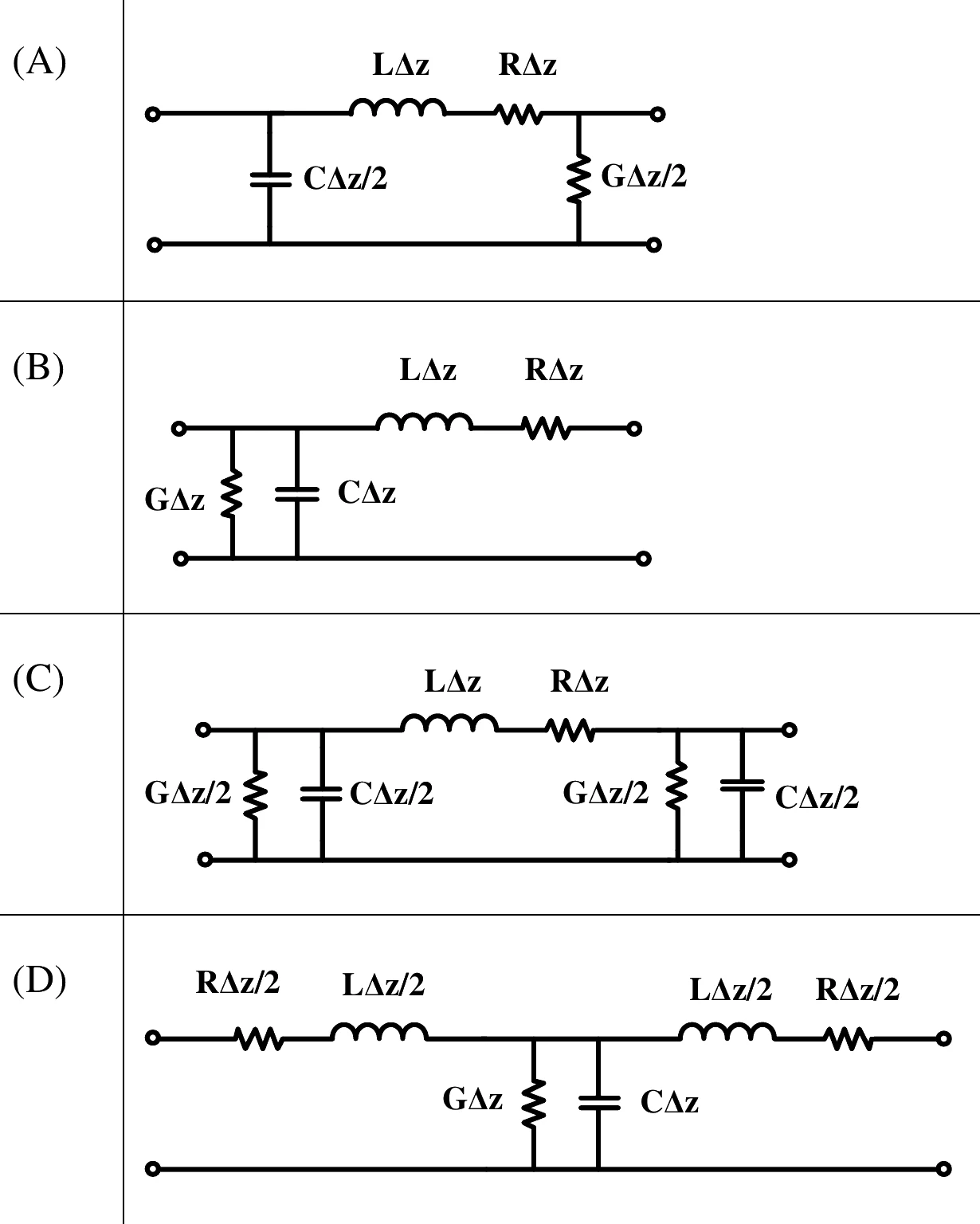
Which of the circuits in the figure represent a lumped-element equivalent of an infinitesimal section of a transmission line?
One or more options are correct.
Full question on page 40 of the official paper (PDF)
Show answerHide answer
Key idea: A section of length \Delta z must contain the full series R\Delta z, L\Delta z and the full shunt G\Delta z, C\Delta z, however they are split.
Official answer: B, C and D
As \Delta z \to 0, it doesn't matter where the shunt elements sit (an L, \pi or T section all reduce to the telegrapher's equations), but the totals must be R\Delta z, L\Delta z, G\Delta z and C\Delta z.
- (A) has only C\Delta z/2 and G\Delta z/2 in total: half the shunt elements. Not valid.
- (B) is an L section with the full shunt elements. Valid.
- (C) is a \pi section: two halves of each shunt element. Valid.
- (D) is a T section: two halves of each series element. Valid.
Options (B), (C) and (D).
Q.55
Engineering Mathematics2 marksNAT
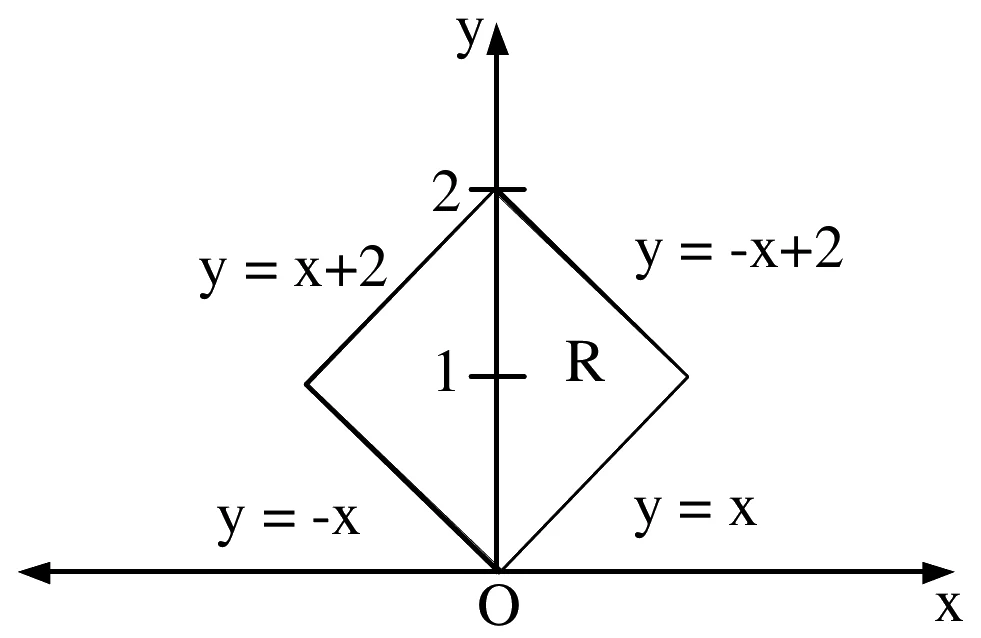
What is the value of over the region in the figure, the square bounded by , , and ?
Answer format: rounded off to the nearest integer
Full question on page 41 of the official paper (PDF)
Show answerHide answer
Key idea: The region is symmetric about the y-axis and xy is odd in x.
Official answer: 0
Replacing x by -x maps R onto itself and changes the sign of xy, so the two halves cancel and the integral is 0.
Directly, for 0 \le y \le 1 the region spans -y \le x \le y, and for 1 \le y \le 2 it spans -(2 - y) \le x \le 2 - y; each inner integral \int x\, dx over a symmetric range is 0. Answer: 0.
Learn the idea:
Q.56
Electronic Devices2 marksNAT
In an extrinsic semiconductor, the hole concentration is , where cm⁻³ is the intrinsic carrier concentration. What ratio of electron to hole mobility makes the hole and electron drift currents equal?
Answer format: rounded off to two decimal places
Full question on page 41 of the official paper (PDF)
Show answerHide answer
Key idea: Equal drift currents in the same field need n\mu_n = p\mu_p, and np = n_i^2.
Official answer: 2.20 to 2.30
The value of n_i cancels. Answer: 2.25.
Learn the idea:
Q.57
Control Systems2 marksNAT
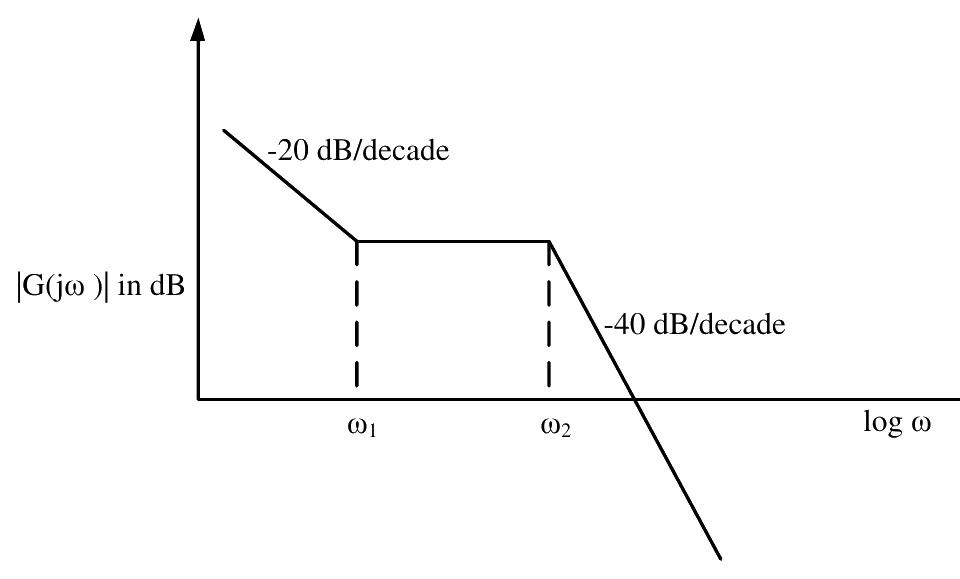
The figure shows the asymptotic magnitude Bode plot of a minimum-phase system: dB/decade up to , flat from to , and dB/decade beyond . Its transfer function is , where , , , , and are positive constants. What is ?
Answer format: rounded off to the nearest integer
Full question on page 41 of the official paper (PDF)
Show answerHide answer
Key idea: Each pole at the origin sets -20 dB/decade from the start; a zero adds +20 and a pole -20 dB/decade at its corner.
Official answer: 4
- -20 dB/decade from the start: one pole at the origin, b = 1.
- At \omega_1 the slope rises by 20 to 0: a single zero, a = 1, z = \omega_1.
- At \omega_2 the slope falls by 40: a double pole, c = 2, p = \omega_2.
So a + b + c = 1 + 1 + 2 = 4.
Learn the idea:
Q.58
Networks, Signals and Systems2 marksNAT
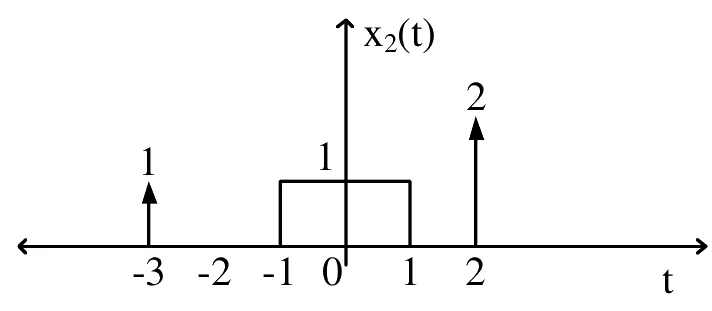
Let , and let be as in the figure. For , what is ?
Answer format: rounded off to the nearest integer
Full question on page 42 of the official paper (PDF)
Show answerHide answer
Key idea: The area of a convolution is the product of the two areas.
Official answer: 15
\int y\, dt = \left(\int x_1\, dt\right)\left(\int x_2\, dt\right)x_1 is a pulse of height 1 and width 3, area 3. x_2 has area 1 + (1 \times 2) + 2 = 5: the two impulses and the pulse. So \int y\, dt = 3 \times 5 = 15.
Q.59
Communications2 marksNAT
is white Gaussian noise with power spectral density W/Hz. It is input to an LTI system with impulse response . What is the average power of the system output, in W?
Answer format: W, rounded off to two decimal places
Full question on page 42 of the official paper (PDF)
Show answerHide answer
Key idea: For white noise of PSD S_0, the output power is S_0 \int |h(t)|^2 dt, by Parseval.
Official answer: 0.24 to 0.26
In the frequency domain, |H(f)|^2 = 1/(1 + 4\pi^2 f^2), whose integral over all f is also \tfrac{1}{2}. Answer: 0.25.
Q.60
Electromagnetics2 marksNAT
A transparent dielectric coating is applied to glass (, ) to eliminate the reflection of red light ( µm). What is the minimum thickness of the coating, in µm?
Answer format: µm, rounded off to two decimal places
Full question on page 42 of the official paper (PDF)
Show answerHide answer
Key idea: A quarter-wave layer cancels reflection when its index is the geometric mean of the media on either side.
Official answer: 0.12 to 0.14
Glass has n = \sqrt{4} = 2 and air n = 1, so the coating needs n_c = \sqrt{1 \times 2} = \sqrt{2} and a thickness of a quarter wavelength in the coating:
Answer: 0.13 µm.
Q.61
Electronic Devices2 marksNAT
In a semiconductor device, the Fermi level is 0.35 eV above the valence band edge. The effective density of states in the valence band at K is cm⁻³. What is the thermal equilibrium hole concentration in silicon at 400 K, in units of cm⁻³? Given at 300 K is 0.026 eV.
Answer format: × 10¹³ cm⁻³, rounded off to two decimal places
Full question on page 42 of the official paper (PDF)
Show answerHide answer
Key idea: p = N_V e^{-(E_F - E_V)/kT}, and both N_V (as T^{3/2}) and kT change with temperature.
Official answer: 60.00 to 70.00
Scale both to 400 K, keeping E_F - E_V = 0.35 eV as the question gives it:
That is 63.4 \times 10^{13} cm⁻³. Answer: about 63.4. Leaving out the T^{3/2} factor gives 41.2, outside the key's range.
Learn the idea:
Q.62
Digital Circuits2 marksNAT
A sample and hold circuit uses a resistive switch and a capacitor with a time constant of 1 µs. How long must the sampling switch stay closed to charge the capacitor adequately to a full-scale voltage of 1 V with 12-bit accuracy, in µs?
Answer format: µs, rounded off to two decimal places
Full question on page 42 of the official paper (PDF)
Show answerHide answer
Key idea: 12-bit accuracy means the remaining error, e^{-t/\tau} of full scale, must fall to 2^{-12}.
Official answer: 8.30 to 8.34
Answer: 8.32 µs. (Asking for half an LSB, 2^{-13}, would give 9.01 µs, which is outside the key's range.)
Learn the idea:
Q.63
Digital Circuits2 marksNAT
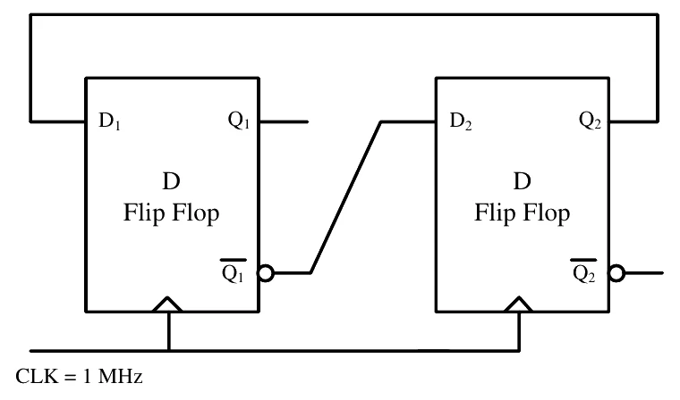
In the sequential circuit in the figure, two D flip-flops share a 1 MHz clock, with and . The initial states are and . What is the frequency of the signal , in kHz?
Answer format: kHz, rounded off to the nearest integer
Full question on page 43 of the official paper (PDF)
Show answerHide answer
Key idea: Step the state (Q_1, Q_2) clock by clock until it repeats; the cycle length divides the clock frequency.
Official answer: 250, or 500
On each edge, Q_1 \leftarrow Q_2 and Q_2 \leftarrow \overline{Q_1}:
The state repeats every 4 clocks, and Q_2 is high for two of them and low for two, so it is a square wave at 1\ \text{MHz}/4 = 250 kHz.
The key accepts 250 or 500. 500 kHz is what you get by reading D_2 as connected to Q_1 instead: then the state alternates (1, 0) \to (0, 1) \to (1, 0), a cycle of 2 clocks. The line in the figure is drawn from the \overline{Q_1} output.
Learn the idea:
Q.64
Analog Circuits2 marksNAT
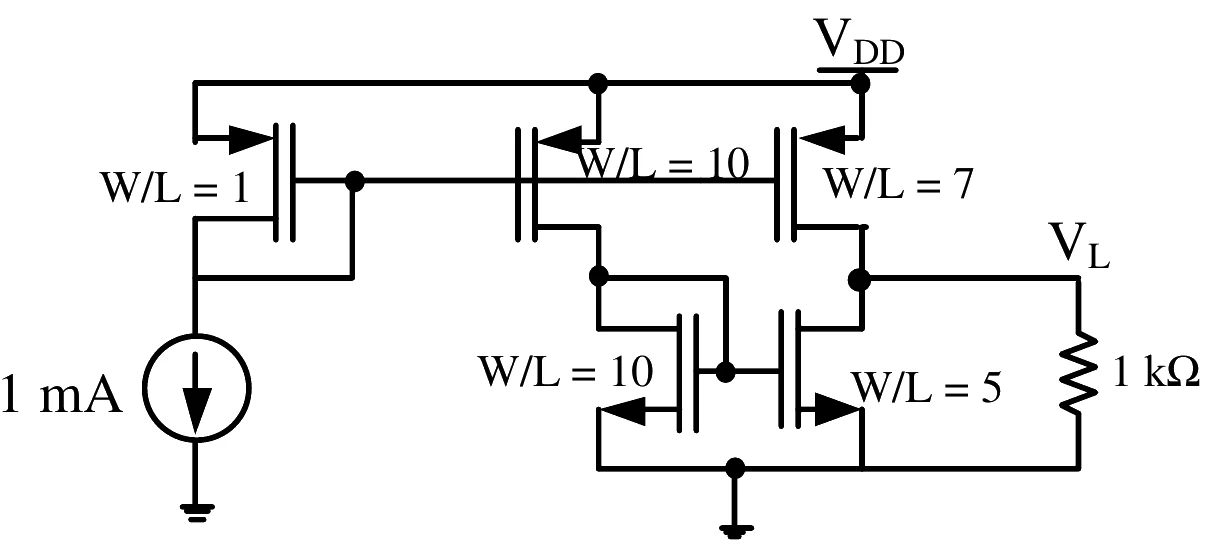
In the circuit in the figure, a 1 mA reference flows through a diode-connected PMOS (W/L = 1). It is mirrored by PMOS devices with W/L = 10 and W/L = 7. The W/L = 10 PMOS feeds a diode-connected NMOS (W/L = 10), which is mirrored by an NMOS with W/L = 5. The output node, where the W/L = 7 PMOS and W/L = 5 NMOS drains meet, drives a 1 kΩ load to ground. What is the voltage , in V?
Answer format: V, rounded off to two decimal places
Full question on page 43 of the official paper (PDF)
Show answerHide answer
Key idea: In saturation, a mirror copies the reference current scaled by the ratio of W/L.
Official answer: 2
- PMOS W/L = 10: 10 \times 1 = 10 mA, into the diode-connected NMOS of W/L = 10.
- NMOS W/L = 5: \tfrac{5}{10} \times 10 = 5 mA, drawn from the output node.
- PMOS W/L = 7: 7 \times 1 = 7 mA, pushed into the output node.
The difference, 7 - 5 = 2 mA, flows through the 1 kΩ, so V_L = 2 \times 1 = 2.00 V, assuming every transistor stays in saturation and channel-length modulation is ignored.
Q.65
Communications2 marksNAT
Eight symbols a to h occur with frequencies , , , , , , and . A symbol is chosen, and it is identified by a series of truthfully answered yes/no questions. What is the average number of questions when they are asked in the most efficient sequence?
Answer format: rounded off to two decimal places
Full question on page 44 of the official paper (PDF)
Show answerHide answer
Key idea: The best question sequence is a Huffman code: each question is one bit.
Official answer: 1.97 to 1.99
Ask "is it a?", then "is it b?", and so on: a takes 1 question, b 2, ..., f 6, and g and h 7 each. This is the Huffman code for these probabilities, so no sequence does better on average:
Every probability is a power of \tfrac{1}{2}, so this equals the entropy exactly. Answer: 1.98.
Sources
- GATE 2023 EC question paper (PDF), published by IIT Kanpur. The questions are theirs: we paraphrase each question and its options, and link to the original.
- GATE 2023 EC answer key (PDF). It was published after the challenge window closed. The provisional key is no longer available, so we can't tell which answers, if any, changed between the two. The key gives marks to all for Q22 and Q46.