GATE EC Digital Circuits Previous Year Questions with Solutions
27 Digital Circuits questions from the GATE EC 2026 and 2025 and 2024 and 2023 papers, newest first. Try each one, then open its answer: the official answer from that year's key and a worked solution. Each question links to its place in the full paper.
GATE 2026, Q.20
Digital Circuits1 markMCQ
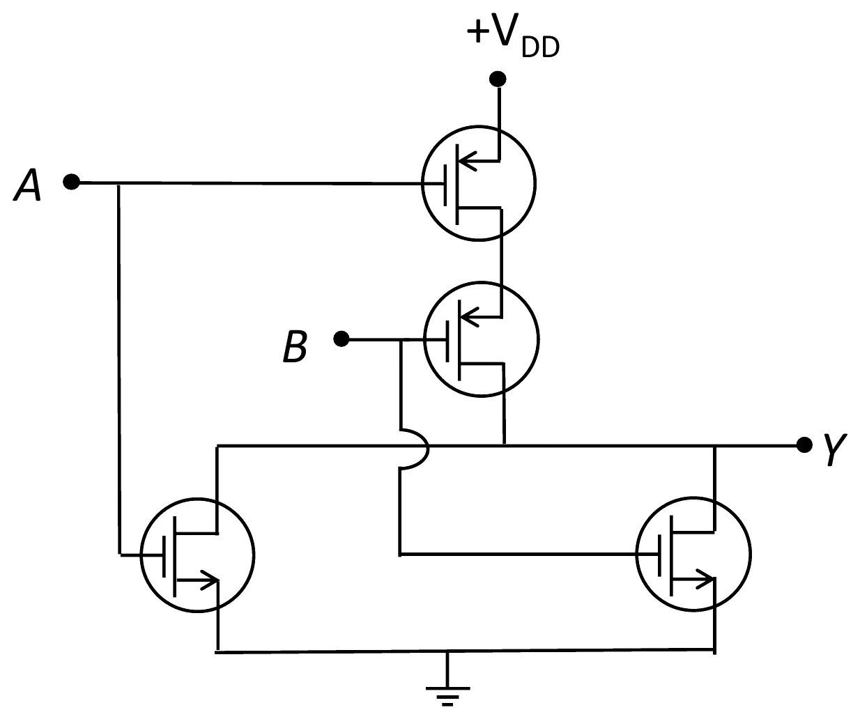
Two PMOS transistors in series pull the output up to VDD, and two NMOS transistors in parallel pull it down, gated by A and B. Which logic function is Y?
Full question on page 20 of the official paper (PDF)
Show answerHide answer
Key idea: Series pull-up and parallel pull-down is the NOR structure.
Official answer: A
The pull-up network (PMOS in series) conducts only when A = 0 and B = 0. The pull-down network (NMOS in parallel) conducts when A = 1 or B = 1.
Y = \overline{A + B}That is NOR. Option (A).
Learn the idea:
GATE 2026, Q.27
Digital Circuits1 markMSQ
How many flip-flops does a binary ripple counter need to count from 0 to 64?
One or more options are correct.
Full question on page 27 of the official paper (PDF)
Show answerHide answer
Key idea: 65 states need 2^n \ge 65.
Official answer: B
Six flip-flops give 2^6 = 64 states, one short of the 65 needed for 0 to 64, so n = 7 (2^7 = 128). Option (B) only.
Learn the idea:
GATE 2026, Q.35
Digital Circuits1 markNAT
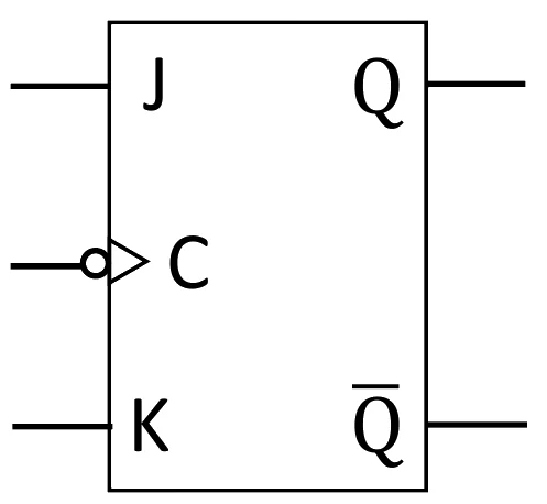
A negative-edge JK flip-flop with J and K tied high is clocked by a 10 Hz square wave. Find the frequency of Q.
Answer format: Hz (cycles per second), rounded off to two decimal places
Full question on page 32 of the official paper (PDF)
Show answerHide answer
Key idea: J = K = 1 toggles Q on every clock edge, halving the frequency.
Official answer: 4.90 to 5.10
The clock has 10 falling edges a second and Q changes on each one, so Q completes 5 cycles a second: 5.00 Hz.
Learn the idea:
GATE 2026, Q.42
Digital Circuits2 marksMCQ
A 256 KB memory starts at address 2500H. What is its last address?
Full question on page 39 of the official paper (PDF)
Show answerHide answer
Key idea: Last address = first address + size - 1, with 256 KB = 40000H.
Official answer: C
256 KB is 256 \times 1024 = 2^{18} byte locations, 40000H in hex, so
Option (C).
GATE 2026, Q.45
Digital Circuits2 marksMCQ
Find the 10's complement of the decimal number 47.
Full question on page 42 of the official paper (PDF)
Show answerHide answer
Key idea: The 10's complement of a two-digit number N is 100 - N.
Official answer: B
For the two-digit number 47:
10^2 - 47 = 53Equivalently, the 9's complement (52) plus 1. Option (B).
GATE 2026, Q.48
Digital Circuits2 marksMCQ
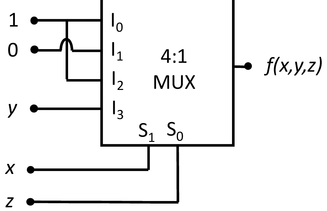
A 4:1 MUX has select lines and and inputs , , , . Find .
Full question on page 45 of the official paper (PDF)
Show answerHide answer
Key idea: Write the MUX output as a sum of select-line minterms times their inputs, then simplify.
Official answer: C
In the figure, I_2 is wired to the same line as I_0 (logic 1), and the 0 line crosses over it to I_1. The MUX output is
The last step uses \bar{z} + z\,(xy) = \bar{z} + xy. Option (C).
Learn the idea:
GATE 2026, Q.49
Digital Circuits2 marksMCQ
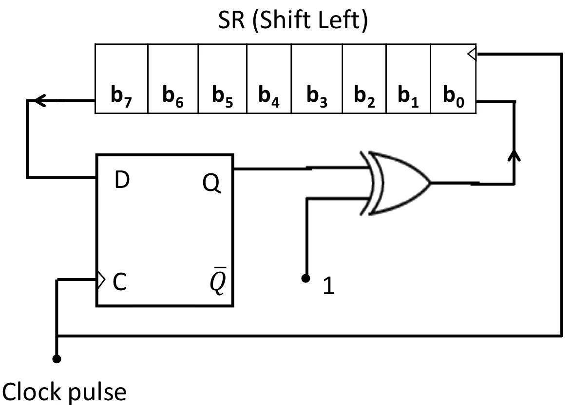
An 8-bit shift-left register feeds into a D flip-flop, and feeds . Starting from all zeros, what does the register hold ( to ) after the 5th rising edge?
Full question on page 46 of the official paper (PDF)
Show answerHide answer
Key idea: The serial input is \bar{Q}, and Q stays 0 until a 1 reaches b_7.
Official answer: A
The serial input to b_0 is Q \oplus 1 = \bar{Q}. On each edge, the register shifts left taking in \bar{Q}, while the flip-flop takes in the old b_7.
| Edge | Q before | Serial in | to after | Q after |
|---|---|---|---|---|
| 1 | 0 | 1 | 00000001 | 0 |
| 2 | 0 | 1 | 00000011 | 0 |
| 3 | 0 | 1 | 00000111 | 0 |
| 4 | 0 | 1 | 00001111 | 0 |
| 5 | 0 | 1 | 00011111 | 0 |
b_7 stays 0 for the first eight edges, so Q stays 0 and a 1 enters every time. Option (A).
Learn the idea:
GATE 2026, Q.56
Digital Circuits2 marksMSQ
, with as MSB. Which expressions equal ?
One or more options are correct.
Full question on page 53 of the official paper (PDF)
Show answerHide answer
Key idea: Group the minterms on a K-map; minterm 14 can be covered two ways.
Official answer: A and D
Plotting the nine minterms gives these groups:
- 0, 2, 8, 10 (the four corners): \bar{x}\bar{z}.
- 5, 7, 13, 15 (x = 1, z = 1): xz.
- 14 is left (w = 1, x = 1, y = 1, z = 0). It pairs with 15 as wxy, or with 10 as wy\bar{z}.
These are options (A) and (D). Option (B) has no term covering minterms 0 and 2 (it gives 0 at w = 0, x = 0, z = 0), and option (C) has no term covering 5 and 7. Options (A) and (D).
Learn the idea:
GATE 2025, Q.23
Digital Circuits1 markMCQ
A 3-input majority gate with inputs , and outputs when two or more inputs are 1, and when two or more are 0. Which expression gives ?
Full question on page 22 of the official paper (PDF)
Show answerHide answer
Key idea: F is 1 exactly when some pair of inputs are both 1.
Official answer: A
Two or more inputs are 1 exactly when at least one of the pairs XY, YZ or ZX is 1, so F = XY + YZ + ZX. Option (A).
The others fail on one row each: X \oplus Y \oplus Z is 0 for X = Y = 1, Z = 0; X + Y + Z is 1 with a single 1; and XYZ is 0 with two 1s.
Learn the idea:
GATE 2025, Q.24
Digital Circuits1 markMCQ
In the circuit in the figure, a full adder takes , and a carry-in of , and its 2-bit output is . With , the circuit works as which of these, with inputs and ?
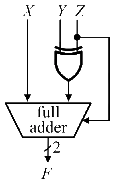
Full question on page 23 of the official paper (PDF)
Show answerHide answer
Key idea: Adding the complement of Y plus 1 is subtracting Y in two's complement.
Official answer: B
With Z = 1, the XOR gives \overline{Y} and the carry-in is 1, so the full adder computes
X + \overline{Y} + 1That is X - Y in two's complement: the sum bit is the difference bit X \oplus Y, and the carry-out is 1 when no borrow is needed (X \ge Y). The circuit is a subtractor. Option (B). With Z = 0 it would add.
Learn the idea:
GATE 2025, Q.35
Digital Circuits1 markNAT
A 4-bit weighted-resistor DAC uses an ideal op-amp with feedback . Bits to (MSB to LSB) switch resistors , , and from V into the inverting input, as in the figure; a switch closes when its bit is 1. By how much does the magnitude of change when the input goes from 1110 to 1101, in mV?
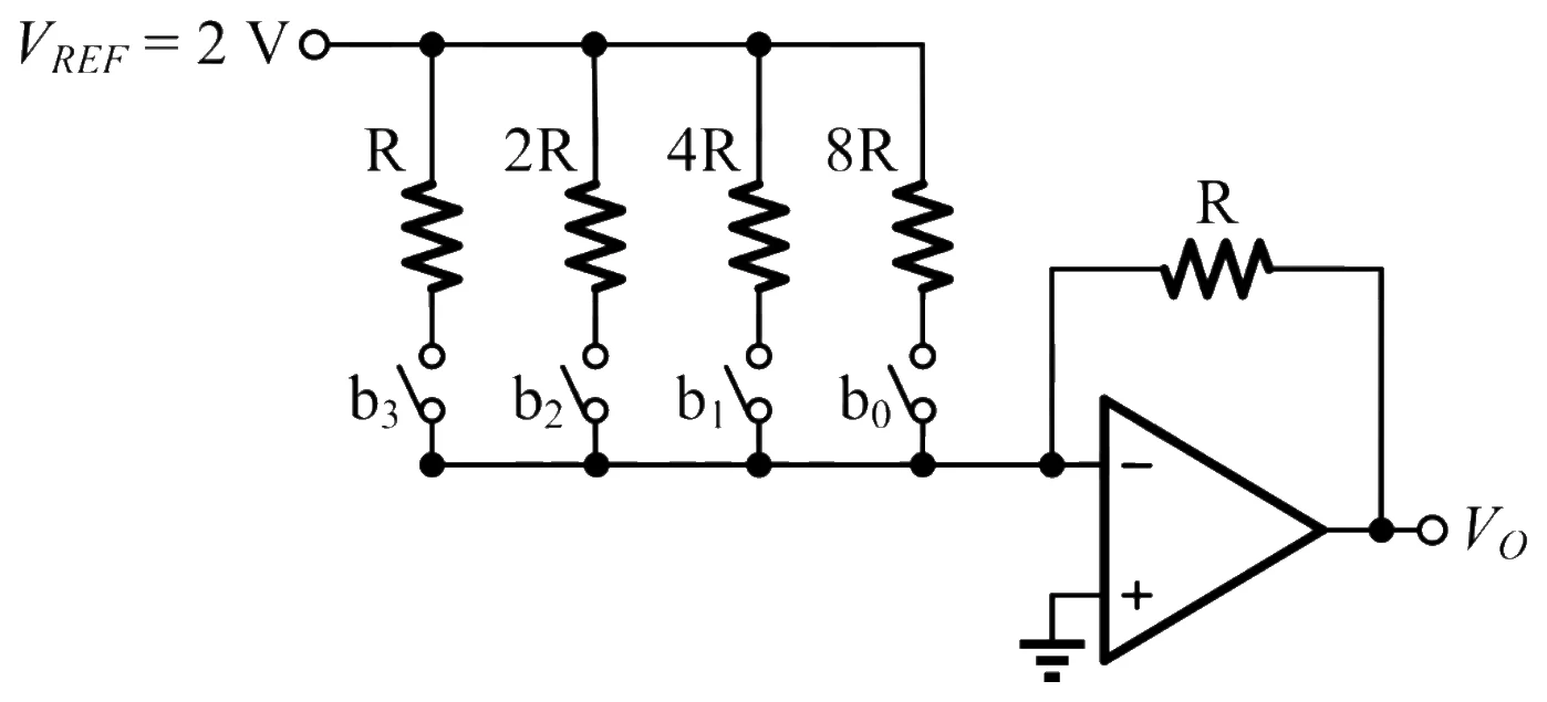
Answer format: mV, rounded off to the nearest integer
Full question on page 30 of the official paper (PDF)
Show answerHide answer
Key idea: Each closed switch adds V_{REF} times the feedback-to-input resistance ratio, so the output is a weighted sum of the bits.
Official answer: 250
V_O = -V_{REF}\left(b_3 + \frac{b_2}{2} + \frac{b_1}{4} + \frac{b_0}{8}\right)- 1110: V_O = -2\,(1 + 0.5 + 0.25) = -3.5 V
- 1101: V_O = -2\,(1 + 0.5 + 0.125) = -3.25 V
The output changes by 0.25 V, that is 250 mV.
Learn the idea:
GATE 2025, Q.44
Digital Circuits2 marksMCQ
A 10-bit ADC samples at 1 MHz with a full-scale voltage of 3.3 V. For a 500 kHz sinusoidal input, what are the maximum SNR (in dB, to two decimal places) and the output data rate (in Mbps)?
Full question on page 39 of the official paper (PDF)
Show answerHide answer
Key idea: A full-scale sine quantized to N bits has an SNR of 6.02N + 1.76 dB, whatever the full-scale voltage.
Official answer: A
The full-scale voltage cancels out of the ratio. Each of the 10^6 samples per second produces 10 bits, so the data rate is 10 Mbps. Option (A).
5 Mbps would come from using the 500 kHz signal frequency instead of the 1 MHz sampling rate.
Learn the idea:
GATE 2025, Q.45
Digital Circuits2 marksMCQ
In the positive-edge-triggered circuit in the figure, the first flip-flop's D comes from a multiplexer choosing (SEL = 1) or (SEL = 0). The second flip-flop's D comes from a multiplexer choosing the first flip-flop's (SEL = 1) or (SEL = 0). is the XOR of the two outputs. With SEL and S as in the timing diagram and no timing violations, what is the sequence of from to ?
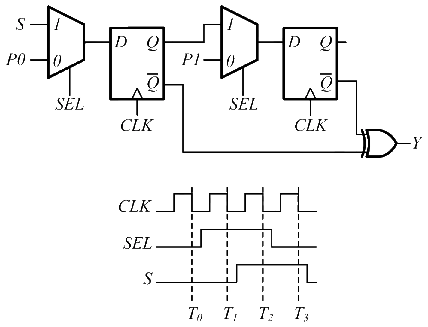
Full question on page 40 of the official paper (PDF)
Show answerHide answer
Key idea: The flip-flops change only on rising clock edges, so read the inputs at each rising edge and the output at the instant after it.
Official answer: A
Y = \overline{Q_1} \oplus \overline{Q_2} = Q_1 \oplus Q_2. The marks T_0 to T_3 are falling edges, so each comes just after a rising edge. At those rising edges:
- Before T_0: SEL = 0, so Q_1 = P_0 = 0 and Q_2 = P_1 = 1. Y = 1.
- Before T_1: SEL = 1, S = 0, so Q_1 = S = 0 and Q_2 takes the old Q_1 = 0. Y = 0.
- Before T_2: SEL = 1, S = 1, so Q_1 = 1 and Q_2 takes the old Q_1 = 0. Y = 1.
- Before T_3: SEL = 0, so Q_1 = 0 and Q_2 = 1. Y = 1.
The sequence is 1011. Option (A). The first edge loads both flip-flops, so their starting state doesn't matter.
Learn the idea:
GATE 2025, Q.62
Digital Circuits2 marksNAT
In the circuit in the figure, the first flip-flop's Q drives the second's D, and the second's Q and an input go through an AND gate back to the first flip-flop's D. The AND gate's propagation delay is 1 ns, and the flip-flops have a set-up time of 2 ns, a hold time of 0 ns and a clock-to-Q delay of 2 ns. What is the maximum clock frequency with no set-up violations, in MHz?
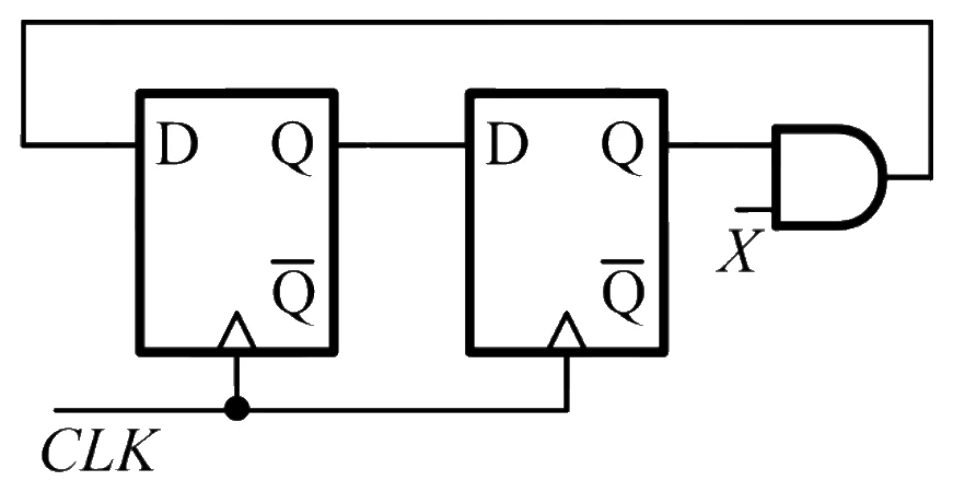
Answer format: MHz, rounded off to the nearest integer
Full question on page 51 of the official paper (PDF)
Show answerHide answer
Key idea: The clock period must cover the slowest register-to-register path: clock-to-Q, then the logic, then set-up.
Official answer: 200
- First flip-flop to second: 2 + 0 + 2 = 4 ns (no logic between them).
- Second flip-flop through the AND gate to the first: 2 + 1 + 2 = 5 ns.
The slower path sets the period, T_{min} = 5 ns, so
Learn the idea:
GATE 2024, Q.19
Digital Circuits1 markMCQ
What are the essential prime implicants of ?
Full question on page 17 of the official paper (PDF)
Show answerHide answer
Key idea: A prime implicant is essential only if it covers some minterm that no other prime implicant covers.
Official answer: A
The prime implicants are \overline{B}\,\overline{D} (0, 2, 8, 10), BD (5, 7, 13, 15), AB (12, 13, 14, 15) and A\overline{D} (8, 10, 12, 14).
- \overline{B}\,\overline{D} is the only one covering 0 and 2: essential.
- BD is the only one covering 5 and 7: essential.
- AB's minterms 12 and 14 are also covered by A\overline{D}, and 13 and 15 by BD, so it is not essential (nor is A\overline{D}).
The essential prime implicants are BD and \overline{B}\,\overline{D}. Option (A).
Learn the idea:
GATE 2024, Q.27
Digital Circuits1 markNAT
A machine has a 32-bit architecture with one-word instructions, 24 registers and 40 instructions. Each instruction has five fields: opcode, two source registers, one destination register and an unsigned immediate value. What is the immediate's maximum value?
Answer format: An integer
Full question on page 23 of the official paper (PDF)
Show answerHide answer
Key idea: Give each field the fewest bits that can name all its values, and the immediate gets whatever is left.
Official answer: 2047
- Opcode: 40 instructions need \lceil\log_2 40\rceil = 6 bits.
- Registers: 24 need \lceil\log_2 24\rceil = 5 bits each, so 15 bits for three.
- Immediate: 32 - 6 - 15 = 11 bits.
The largest unsigned 11-bit value is 2^{11} - 1 = 2047.
GATE 2024, Q.29
Digital Circuits1 markNAT
In a number system of base , the equation has as one of its solutions. What is ?
Answer format: An integer
Full question on page 24 of the official paper (PDF)
Show answerHide answer
Key idea: Rewrite the coefficients 12 and 37 as base-r numerals, then substitute the root.
Official answer: 11
In base r, the numeral 12 means r + 2 and 37 means 3r + 7. Substituting x = 8:
The digits 7 and 8 need a base above 8, which r = 11 is. The other root is 13 - 8 = 5 in decimal, since the roots add to r + 2 = 13.
GATE 2024, Q.40
Digital Circuits2 marksMCQ
A 4-bit priority encoder has inputs , , , in descending priority, and outputs for , , , respectively. What is the expression for ?
Full question on page 30 of the official paper (PDF)
Show answerHide answer
Key idea: B is 1 for the codes 01 and 11, that is when D_2 wins or when D_0 wins.
Official answer: B
D_2 wins when D_3 = 0 and D_2 = 1. D_0 wins when D_3 = D_2 = D_1 = 0 (with at least one input active, D_0 must then be 1). So
Option (B).
Learn the idea:
GATE 2024, Q.41
Digital Circuits2 marksMCQ
In the circuit in the figure, a 2 × 1 MUX with a propagation delay of 10 ns has its output fed back to input 0 directly and to input 1 through an inverter with zero delay. If , what is ?
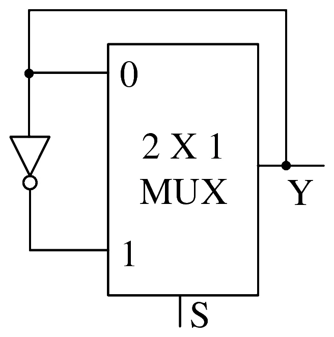
Full question on page 31 of the official paper (PDF)
Show answerHide answer
Key idea: With S = 1 the MUX passes its own inverted output, so Y flips once per propagation delay.
Official answer: B
With S = 1, Y(t) = \overline{Y(t - 10\ \text{ns})}: every 10 ns the output takes the opposite of its value 10 ns earlier. So it flips every 10 ns, a square wave of period 20 ns.
f = \frac{1}{20\ \text{ns}} = 50\ \text{MHz}Option (B). One half-period is one delay, which is why it isn't 100 MHz.
Learn the idea:
GATE 2024, Q.42
Digital Circuits2 marksMCQ
In the synchronous circuit in the figure, and , each formed by an OR gate. What is the sequence of states ?
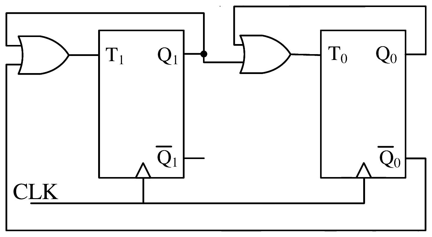
Full question on page 32 of the official paper (PDF)
Show answerHide answer
Key idea: A T flip-flop toggles when T = 1 and holds when T = 0, so work out both T inputs from the present state.
Official answer: B
- 11: T_1 = 1, T_0 = 1, both toggle: 00.
- 00: T_1 = 0 + 1 = 1, T_0 = 0: 10.
- 10: T_1 = 1, T_0 = 1: 01.
- 01: T_1 = 0 + 0 = 0, T_0 = 1: 00.
From 11 the circuit runs 11 → 00 → 10 → 01 → 00 and then repeats 00 → 10 → 01. Option (B).
Learn the idea:
GATE 2024, Q.46
Digital Circuits2 marksMCQ
A full-scale sine is applied to a 10-bit ADC. The fundamental at the output has a normalised power of 1 W, and the total noise and distortion is 10 µW. What is the effective number of bits, to the nearest integer?
Full question on page 35 of the official paper (PDF)
Show answerHide answer
Key idea: Measure SINAD in dB and invert the ideal-ADC formula 6.02N + 1.76.
Official answer: B
To the nearest integer, 8. Option (B). The noise and distortion cost the converter about two of its ten bits.
GATE 2023, Q.23
Digital Circuits1 markMCQ
In the circuit in the figure, P and Q are the inputs of a 2 × 1 multiplexer: is grounded, and the select line is Q. What logical function does it realise?
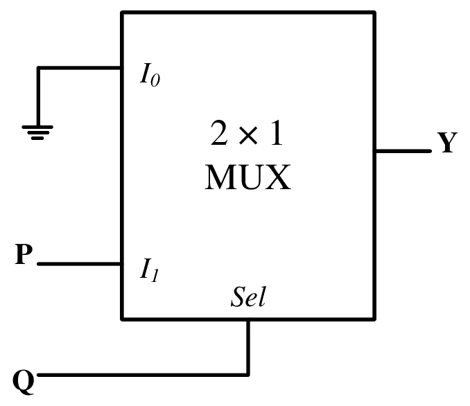
Full question on page 16 of the official paper (PDF)
Show answerHide answer
Key idea: A 2 × 1 multiplexer gives Y = \bar{S} I_0 + S I_1.
Official answer: A
Y = \bar{Q} \cdot 0 + Q \cdot P = PQY is 1 only when Q selects I_1 and P is 1: an AND gate. Option (A).
Learn the idea:
GATE 2023, Q.24
Digital Circuits1 markMCQ
The synchronous sequential circuit in the figure, three D flip-flops in a chain sharing one clock, works at a clock frequency of 1 GHz. What are its throughput, in Mbits/s, and its latency, in ns?
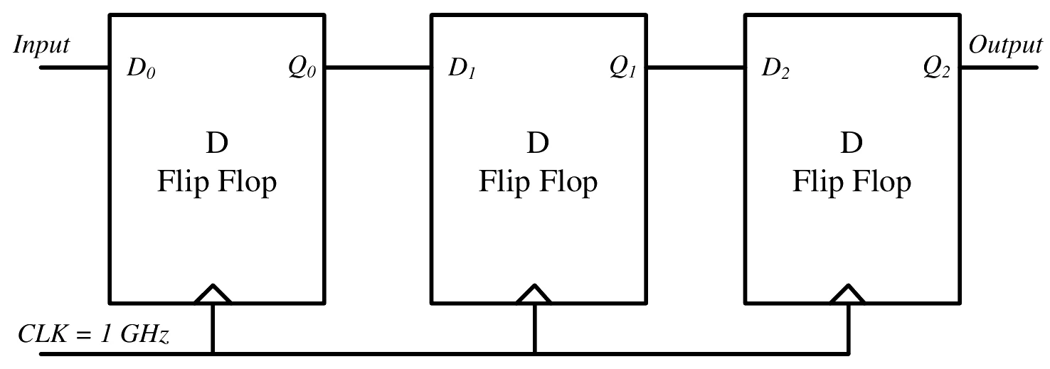
Full question on page 17 of the official paper (PDF)
Show answerHide answer
Key idea: A new bit enters on every clock edge, and each bit needs one clock per flip-flop to reach the output.
Official answer: A
Like a pipeline, the chain accepts one new bit every clock period of 1 ns, so its throughput is one bit per ns, 1000 Mbit/s.
Each bit moves one flip-flop per clock, so it appears at Q_2 three clocks after it enters: a latency of 3 ns. Option (A).
Learn the idea:
GATE 2023, Q.31
Digital Circuits1 markNAT
The signal-to-noise ratio (SNR) of an ADC with a full-scale sinusoidal input is 61.96 dB. What is the resolution of the ADC, in bits?
Answer format: bits, rounded off to the nearest integer
Full question on page 21 of the official paper (PDF)
Show answerHide answer
Key idea: For an ideal N-bit ADC and a full-scale sine, \text{SNR} = 6.02N + 1.76 dB.
Official answer: 10
The formula comes from a full-scale sine's power, (2^N \Delta)^2/8, over the quantisation noise power, \Delta^2/12: their ratio is 1.5 \times 4^N, which is 1.76 + 6.02N dB. Answer: 10 bits.
Learn the idea:
GATE 2023, Q.34
Digital Circuits1 markNAT
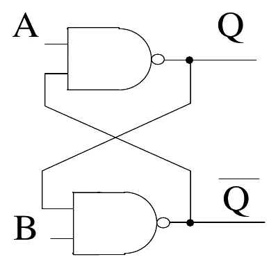
For the circuit in the figure, two cross-coupled NAND gates with inputs A and B and outputs Q and , the propagation delay of each NAND gate is 1 ns. What is the critical path delay, in ns?
Answer format: ns, rounded off to the nearest integer
Full question on page 23 of the official paper (PDF)
Show answerHide answer
Key idea: A change only settles once it has gone through one gate and been fed back through the other.
Official answer: 2
Pull A low to set the latch: after 1 ns the first gate's output Q goes high. Only then does the second gate see the new Q, and after another 1 ns \overline{Q} goes low and holds Q. The outputs are settled after two gate delays, so the critical path is 2 ns.
Learn the idea:
GATE 2023, Q.62
Digital Circuits2 marksNAT
A sample and hold circuit uses a resistive switch and a capacitor with a time constant of 1 µs. How long must the sampling switch stay closed to charge the capacitor adequately to a full-scale voltage of 1 V with 12-bit accuracy, in µs?
Answer format: µs, rounded off to two decimal places
Full question on page 42 of the official paper (PDF)
Show answerHide answer
Key idea: 12-bit accuracy means the remaining error, e^{-t/\tau} of full scale, must fall to 2^{-12}.
Official answer: 8.30 to 8.34
Answer: 8.32 µs. (Asking for half an LSB, 2^{-13}, would give 9.01 µs, which is outside the key's range.)
Learn the idea:
GATE 2023, Q.63
Digital Circuits2 marksNAT
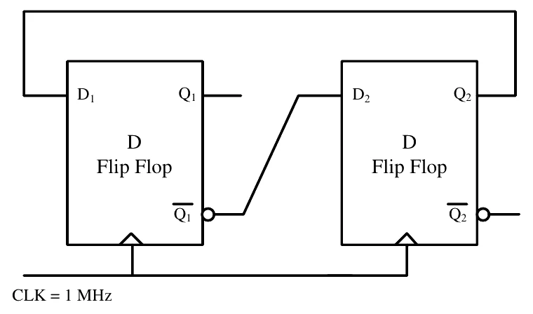
In the sequential circuit in the figure, two D flip-flops share a 1 MHz clock, with and . The initial states are and . What is the frequency of the signal , in kHz?
Answer format: kHz, rounded off to the nearest integer
Full question on page 43 of the official paper (PDF)
Show answerHide answer
Key idea: Step the state (Q_1, Q_2) clock by clock until it repeats; the cycle length divides the clock frequency.
Official answer: 250, or 500
On each edge, Q_1 \leftarrow Q_2 and Q_2 \leftarrow \overline{Q_1}:
The state repeats every 4 clocks, and Q_2 is high for two of them and low for two, so it is a square wave at 1\ \text{MHz}/4 = 250 kHz.
The key accepts 250 or 500. 500 kHz is what you get by reading D_2 as connected to Q_1 instead: then the state alternates (1, 0) \to (0, 1) \to (1, 0), a cycle of 2 clocks. The line in the figure is drawn from the \overline{Q_1} output.
Learn the idea: