GATE EC Electronic Devices Previous Year Questions with Solutions
21 Electronic Devices questions from the GATE EC 2026 and 2025 and 2024 and 2023 papers, newest first. Try each one, then open its answer: the official answer from that year's key and a worked solution. Each question links to its place in the full paper.
GATE 2026, Q.14
Electronic Devices1 markMCQ
Which carrier transport mechanism dominates the current in a Zener diode in breakdown?
Full question on page 14 of the official paper (PDF)
Show answerHide answer
Key idea: A heavily doped junction is thin enough for band-to-band tunnelling.
Official answer: C
In reverse breakdown, the field across a Zener diode's very thin depletion region is strong enough for electrons to tunnel straight from the valence band on the p side to the conduction band on the n side. That tunnelling carries the current. Option (C).
Avalanche breakdown, in lightly doped junctions at higher voltages, works by impact ionisation instead; the question asks about the Zener mechanism.
Learn the idea:
GATE 2026, Q.25
Electronic Devices1 markMSQ
A p-n junction is forward biased at 2 V. What is the separation between the quasi-Fermi levels and ?
One or more options are correct.
Full question on page 25 of the official paper (PDF)
Show answerHide answer
Key idea: An applied bias V splits the quasi-Fermi levels by qV.
Official answer: A
At a forward bias of 2 V the split is q \times 2 V = 2 eV, option (A).
Options (C) and (D) give an energy in volts, which isn't an energy unit, and 1 eV doesn't match the bias. The official key lists (A) only.
Learn the idea:
GATE 2026, Q.29
Electronic Devices1 markMSQ
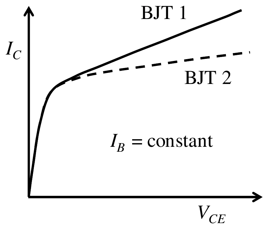
Two BJTs at the same base current: in the active region, BJT 1's collector current rises more steeply with VCE than BJT 2's. Compare their Early voltages |VA1| and |VA2|.
One or more options are correct.
Full question on page 29 of the official paper (PDF)
Show answerHide answer
Key idea: The active-region slope is about I_C/|V_A|: the steeper curve has the smaller Early voltage.
Official answer: C and D
Compare the two active-region slopes at the same I_C:
- BJT 1 is steeper, so |V_{A1}| < |V_{A2}|: option (C).
- BJT 2 still has a nonzero slope, so |V_{A2}| is finite: option (D).
- BJT 1 has the steeper slope, so its Early voltage is certainly not infinite, which rules out (B), and (A) is the reverse of (C).
Learn the idea:
GATE 2026, Q.54
Electronic Devices2 marksMSQ
An LED uses a direct-gap semiconductor with eV ( J s, m/s). In which wavelength bands will it not emit?
One or more options are correct.
Full question on page 51 of the official paper (PDF)
Show answerHide answer
Key idea: An LED emits in a narrow band just above the gap, at \lambda \approx hc/E_g.
Official answer: A, B and D
The peak wavelength is set by the bandgap:
- 1410 nm (0.88 eV) and 1090 nm (1.14 eV) need photons below the gap. No transition gives them, so no emission: (A) and (B).
- 950 ± 20 nm contains 956 nm: the LED emits here.
- 510 nm (2.43 eV) is more than 1 eV above the gap. Carriers relax to the band edges before recombining, so the emission band (a few kT wide) doesn't reach it: (D).
Options (A), (B) and (D).
Learn the idea:
GATE 2026, Q.64
Electronic Devices2 marksNAT
Electron concentration falls linearly from cm⁻³ at µm to cm⁻³ at µm. With cm²/V s, mV and C, find the electron diffusion current density.
Answer format: A/mm², rounded off to two decimal places (the key accepts either sign)
Full question on page 58 of the official paper (PDF)
Show answerHide answer
Key idea: J_n = qD_n\,dn/dx, with D_n = \mu_n V_T from Einstein's relation.
Official answer: -36.50 to -34.50, or 34.50 to 36.50
Einstein's relation gives the diffusion coefficient:
The gradient, over 3\ \mum = 3 \times 10^{-4} cm:
Electrons diffuse towards +x, so the conventional current flows towards -x. Its magnitude is about 35.47 A/mm².
Note: The official key accepts either sign: -36.50 to -34.50 or 34.50 to 36.50. The question asks for the current density without fixing a positive direction.
Learn the idea:
GATE 2025, Q.31
Electronic Devices1 markMSQ
Which of these can be used as an n-type dopant for silicon?
One or more options are correct.
Full question on page 29 of the official paper (PDF)
Show answerHide answer
Key idea: An n-type dopant has one more valence electron than silicon: it comes from group 15.
Official answer: A and D
Silicon has four valence electrons. Arsenic and phosphorus (group 15) have five, so each donates a free electron: they are donors, and make silicon n-type.
Boron and gallium (group 13) have three and accept an electron, making silicon p-type. Options (A) and (D).
Learn the idea:
GATE 2025, Q.46
Electronic Devices2 marksMCQ
A semiconductor has intrinsic carrier concentration m⁻³ at 300 K, and electron and hole mobilities of 0.15 and 0.05 m²/Vs. With C, what is its intrinsic resistivity at 300 K, in kΩ·m?
Full question on page 41 of the official paper (PDF)
Show answerHide answer
Key idea: In an intrinsic semiconductor both carriers have concentration n_i, so their mobilities add.
Official answer: B
Option (B).
GATE 2025, Q.48
Electronic Devices2 marksMCQ
The electron mobility in non-degenerate germanium at 300 K is 0.38 m²/Vs. With J/K and C, what is the electron diffusivity at 300 K, in cm²/s, to the nearest integer?
Full question on page 43 of the official paper (PDF)
Show answerHide answer
Key idea: The Einstein relation ties diffusivity to mobility through the thermal voltage kT/e.
Official answer: B
To the nearest integer, 98. Option (B). Forgetting that 1 m² is 10^4 cm² gives 0.0098, and 26 is the thermal voltage in mV.
Learn the idea:
GATE 2025, Q.63
Electronic Devices2 marksNAT
An ideal germanium p-n junction diode has a reverse saturation current of 10 µA at 300 K. With J/K and C, what forward voltage gives a current of 100 mA at 300 K, in volts?
Answer format: Volts, rounded off to two decimal places
Full question on page 52 of the official paper (PDF)
Show answerHide answer
Key idea: Invert the ideal diode equation: the voltage grows with the logarithm of the current ratio.
Official answer: 0.23 to 0.24
To two decimal places, 0.24 V, inside the key's range of 0.23 to 0.24.
Learn the idea:
GATE 2024, Q.22
Electronic Devices1 markMCQ
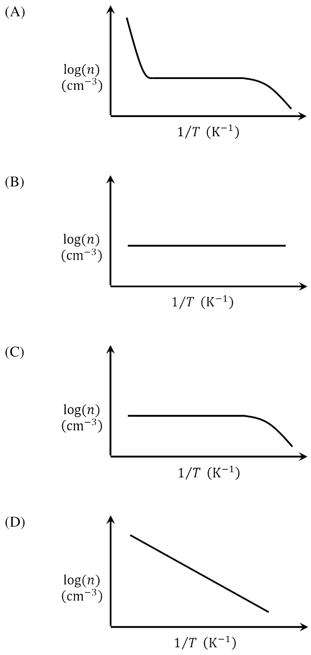
For non-degenerately doped n-type silicon, which plot in the figure shows how the free electron concentration depends on temperature ? Each plots against .
Full question on page 19 of the official paper (PDF)
Show answerHide answer
Key idea: Read the axis backwards: small 1/T is high temperature, so the plot runs from the intrinsic region on the left to freeze-out on the right.
Official answer: A
Going from high to low temperature, left to right along 1/T:
- High T (small 1/T): intrinsic carriers outnumber the donors, and n \approx n_i rises steeply with T.
- Middle range: every donor is ionised, so n \approx N_D, a flat plateau.
- Low T (large 1/T): freeze-out, as electrons drop back onto the donors, so n falls.
Only plot (A) has all three regions. Plot (C) misses the intrinsic rise, (B) has only the plateau, and (D) only a single slope. Option (A).
Learn the idea:
GATE 2024, Q.26
Electronic Devices1 markMSQ
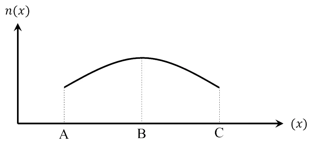
The figure shows the equilibrium free-electron concentration in a doped semiconductor, rising from A to a maximum at B and falling to C. Which statements are true?
One or more options are correct.
Full question on page 23 of the official paper (PDF)
Show answerHide answer
Key idea: At equilibrium the drift and diffusion currents cancel everywhere, and electron current flows opposite to electron motion.
Official answer: A, B and C
- Between B and C, electrons diffuse from B (high n) towards C. Electrons carry negative charge, so the diffusion current points from C to B: (A) true.
- Between A and B, electrons diffuse from B towards A, so the diffusion current points from A to B. At equilibrium drift cancels it, so the drift current points from B to A: (B) true.
- Between B and C, the drift current must point from B to C to cancel diffusion. Electron drift current is along the field, so the field points from B to C: (C) true.
- The same reasoning between A and B puts the field from B to A, so (D) is false.
Options (A), (B) and (C).
Learn the idea:
GATE 2024, Q.52
Electronic Devices2 marksMSQ
Which statements about a BJT's DC current gain are true?
One or more options are correct.
Full question on page 40 of the official paper (PDF)
Show answerHide answer
Key idea: \beta peaks at moderate current: it is pulled down by recombination at low current and by high injection at high current.
Official answer: A, C and D
- (A) True: at high injection the base's majority carriers are no longer negligible, emitter efficiency drops, and \beta falls as I_C rises.
- (B) False: when recombination current in the emitter-base junction dominates the base current, it grows more slowly than I_C, so \beta rises with I_C in this region.
- (C) True: in saturation the base current exceeds I_C/\beta_F, so the ratio I_C/I_B is below the active-region \beta.
- (D) True: avalanche multiplication is amplified by the transistor's gain, so BV_{CEO} \approx BV_{CBO}/\beta^{1/n} falls as \beta rises.
Options (A), (C) and (D).
Learn the idea:
GATE 2024, Q.61
Electronic Devices2 marksNAT
A MOS capacitor on p-type silicon has a 100 nm oxide of relative permittivity 4, a fixed positive oxide charge of C/cm² at the oxide-silicon interface, and a metal work function of 4.6 eV, with F/cm. If the flatband voltage is 0 V, what is the work function of the silicon, in eV?
Answer format: eV, rounded off to two decimal places
Full question on page 45 of the official paper (PDF)
Show answerHide answer
Key idea: The flatband voltage is the work-function difference minus the oxide charge's voltage, V_{FB} = \phi_{ms} - Q_{ox}/C_{ox}.
Official answer: 4.10 to 4.50
With V_{FB} = 0, \phi_m - \phi_s = 0.283 V, so
Within the key's range of 4.10 to 4.50.
GATE 2024, Q.63
Electronic Devices2 marksNAT
In a non-degenerate n-type semiconductor, 5% of the dopant atoms are neutral. The Fermi level is 0.25 eV below , the donor level has degeneracy 2, and the thermal voltage is 20 mV. What is , in eV?
Answer format: eV, rounded off to two decimal places
Full question on page 46 of the official paper (PDF)
Show answerHide answer
Key idea: The fraction of donors still holding their electron follows a Fermi function with the degeneracy factor in front of the exponential.
Official answer: 0.17 to 0.19
Learn the idea:
GATE 2024, Q.64
Electronic Devices2 marksNAT
An NMOS in the linear region carries µA at V. Keeping fixed, is raised to 1.5 V. With µA/V², what is the transconductance at the new operating point, in µA/V?
Answer format: µA/V, rounded off to two decimal places
Full question on page 46 of the official paper (PDF)
Show answerHide answer
Key idea: Use the first point to find the overdrive voltage, then check which region the new V_{DS} puts the device in.
Official answer: 52.40 to 52.60
In the linear region I_{DS} = k\left[V_{ov}V_{DS} - V_{DS}^2/2\right]:
At V_{DS} = 1.5 V > V_{ov}, the transistor is in saturation, where g_m = k V_{ov}:
Using the linear-region expression g_m = kV_{DS} instead would give 75, the usual slip.
GATE 2024, Q.65
Electronic Devices2 marksNAT
A PN-junction solar cell has a photocurrent of 1 mA, and its maximum power point is at 0.3 V. With a thermal voltage of 30 mV, what is the diode's reverse saturation current, in nA?
Answer format: nA, rounded off to two decimal places
Full question on page 46 of the official paper (PDF)
Show answerHide answer
Key idea: At the maximum power point, the derivative of P = VI with respect to V is zero.
Official answer: 4.00 to 4.26
Learn the idea:
GATE 2023, Q.16
Electronic Devices1 markMCQ
In a semiconductor, if the Fermi energy level lies in the conduction band, the semiconductor is known as
Full question on page 11 of the official paper (PDF)
Show answerHide answer
Key idea: A Fermi level near the conduction band means n-type; one inside a band means degenerate doping.
Official answer: A
Doping with donors pushes E_F up towards E_C. Very heavy donor doping pushes it past E_C into the conduction band, where Boltzmann statistics no longer hold: the semiconductor is degenerate. Option (A).
A degenerate p-type semiconductor has E_F inside the valence band instead.
Learn the idea:
GATE 2023, Q.17
Electronic Devices1 markMCQ
For an intrinsic semiconductor at temperature K, which of the following statements is true?
Full question on page 12 of the official paper (PDF)
Show answerHide answer
Key idea: At 0 K no electron has the thermal energy to cross the band gap.
Official answer: A
At 0 K the Fermi function is a step at E_F, which lies in the gap: every state below it is full and every state above it is empty. So the valence band is full and the conduction band is empty, which is why an intrinsic semiconductor is an insulator at 0 K. Option (A).
GATE 2023, Q.19
Electronic Devices1 markMCQ
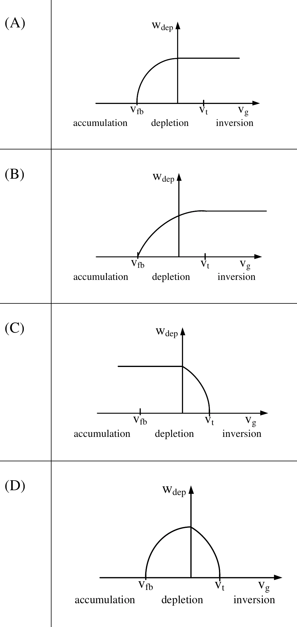
For a MOS capacitor, and are the flat-band and threshold voltages. Which graph in the figure best represents the depletion width as the gate voltage varies?
Full question on page 13 of the official paper (PDF)
Show answerHide answer
Key idea: There is no depletion layer in accumulation; it grows through depletion and stops growing once the inversion layer forms.
Official answer: B
Below V_{fb} (accumulation) majority carriers pile up at the surface and W_{dep} = 0. Between V_{fb} and V_t the depletion layer widens as V_g rises. At V_t the inversion layer forms and screens any further charge, so W_{dep} stays at its maximum, W_{max}, through inversion.
Graph (B) shows exactly this: zero, a smooth rise through depletion, and a flat line beyond V_t. (A) saturates before V_t, and (C) and (D) fall to zero at V_t. Option (B).
GATE 2023, Q.56
Electronic Devices2 marksNAT
In an extrinsic semiconductor, the hole concentration is , where cm⁻³ is the intrinsic carrier concentration. What ratio of electron to hole mobility makes the hole and electron drift currents equal?
Answer format: rounded off to two decimal places
Full question on page 41 of the official paper (PDF)
Show answerHide answer
Key idea: Equal drift currents in the same field need n\mu_n = p\mu_p, and np = n_i^2.
Official answer: 2.20 to 2.30
The value of n_i cancels. Answer: 2.25.
Learn the idea:
GATE 2023, Q.61
Electronic Devices2 marksNAT
In a semiconductor device, the Fermi level is 0.35 eV above the valence band edge. The effective density of states in the valence band at K is cm⁻³. What is the thermal equilibrium hole concentration in silicon at 400 K, in units of cm⁻³? Given at 300 K is 0.026 eV.
Answer format: × 10¹³ cm⁻³, rounded off to two decimal places
Full question on page 42 of the official paper (PDF)
Show answerHide answer
Key idea: p = N_V e^{-(E_F - E_V)/kT}, and both N_V (as T^{3/2}) and kT change with temperature.
Official answer: 60.00 to 70.00
Scale both to 400 K, keeping E_F - E_V = 0.35 eV as the question gives it:
That is 63.4 \times 10^{13} cm⁻³. Answer: about 63.4. Leaving out the T^{3/2} factor gives 41.2, outside the key's range.
Learn the idea: