GATE EC Analog Circuits Previous Year Questions with Solutions
28 Analog Circuits questions from the GATE EC 2026 and 2025 and 2024 and 2023 papers, newest first. Try each one, then open its answer: the official answer from that year's key and a worked solution. Each question links to its place in the full paper.
GATE 2026, Q.17
Analog Circuits1 markMCQ
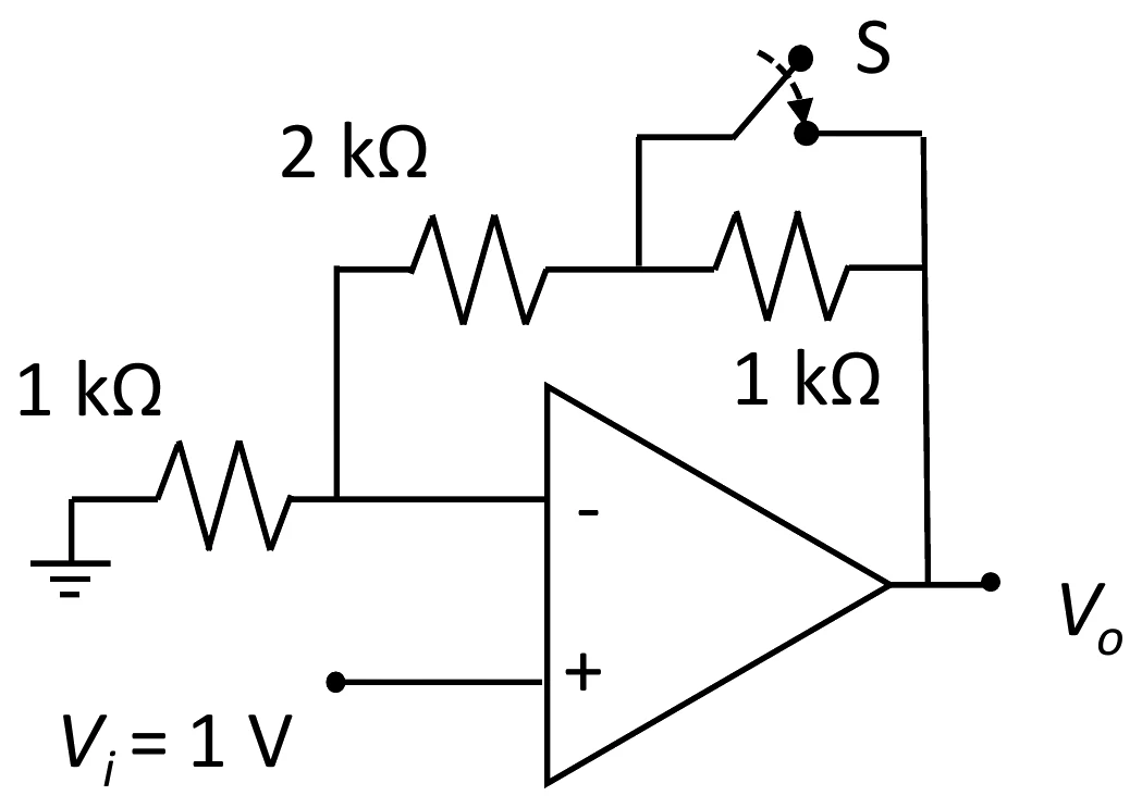
A non-inverting op-amp stage has 1 kΩ from the inverting input to ground and, as feedback, 2 kΩ in series with 1 kΩ, with a switch S across the 1 kΩ. With S open the output is . Find with S closed.
Full question on page 17 of the official paper (PDF)
Show answerHide answer
Key idea: A non-inverting gain is 1 + R_f/R_g; closing S removes 1 kΩ from R_f.
Official answer: C
Take the two switch positions in turn, with R_g = 1 kΩ.
- Switch open: R_f = 3 kΩ, gain 4, so x = 4V_i.
- Switch closed: the 1 kΩ is shorted, R_f = 2 kΩ, gain 3, so V_o = 3V_i.
V_o = \tfrac{3}{4}x. Option (C).
Learn the idea:
GATE 2026, Q.18
Analog Circuits1 markMCQ
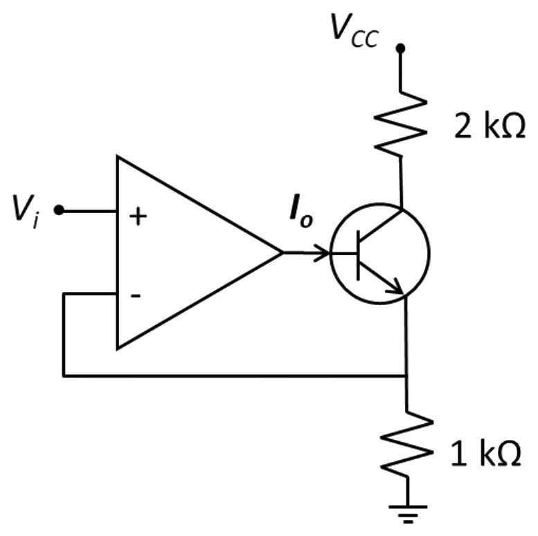
An op-amp drives a BJT's base and senses the voltage across its 1 kΩ emitter resistor, with V at the op-amp input and V. With V and , find the base current .
Full question on page 18 of the official paper (PDF)
Show answerHide answer
Key idea: Feedback holds the emitter at V_i, which fixes I_E; then I_B = I_E/(\beta + 1).
Official answer: D
The emitter sits at V_i = 3 V, across the 1 kΩ resistor. So
Check the BJT is active: V_C = 12 - 2\text{ k}\Omega \times 2.97\text{ mA} \approx 6.06 V, above the emitter. Option (D).
Learn the idea:
GATE 2026, Q.50
Analog Circuits2 marksMCQ
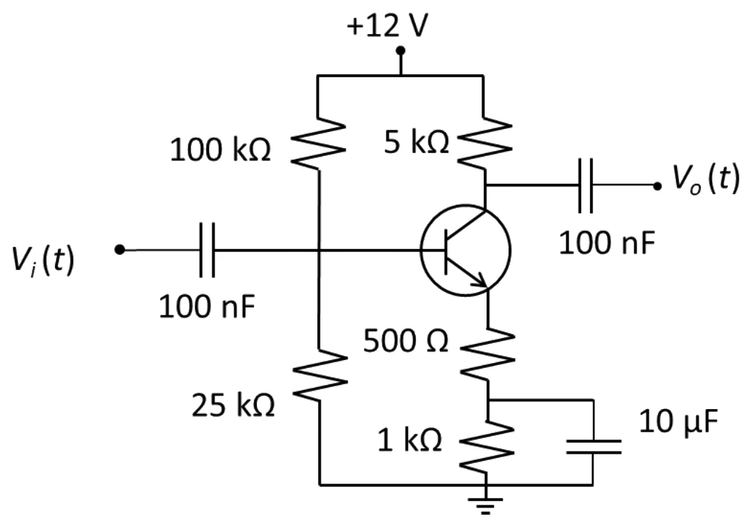
A voltage-divider biased common-emitter stage (100 kΩ and 25 kΩ divider, 5 kΩ collector, 500 Ω unbypassed and 1 kΩ bypassed in the emitter, 12 V supply, , V) is driven by . Which is the best approximation of ?
Full question on page 47 of the official paper (PDF)
Show answerHide answer
Key idea: The capacitors are shorts at both frequencies, so both tones see the same gain \approx -R_C/(r_e + 500).
Official answer: A
Bias. The divider gives a Thévenin source of 12 \times 25/125 = 2.4 V behind 100\,\|\,25 = 20 kΩ. With I_B = I_E/100 and 1.5 kΩ in the emitter:
Capacitors. At \omega = 10^5 rad/s, the 10 µF bypass is 1 Ω against 1 kΩ, and the 100 nF input capacitor is 100 Ω against an input resistance of about 14.5 kΩ. At 10^7 rad/s they are smaller still. Both act as shorts at both frequencies, and the output capacitor carries no current into an open output.
Gain. Only the 500 Ω stays in the emitter for signals:
The same gain applies to both tones, with no phase shift between them, so
The nearest is option (A). Option (C), -190.4, is the gain with the 500 Ω bypassed as well, which the circuit doesn't do.
Note: The exact gain is -9.40, not the option's -9.1. The 500 Ω makes the transistor's output resistance far larger than r_o = 100 V/1 mA, so r_o barely matters. The option's value comes from putting r_o straight across R_C: (5\text{ k}\,\|\,100\text{ k})/525 \approx 9.07. Either way, (A) is the nearest option.
Learn the idea:
GATE 2026, Q.53
Analog Circuits2 marksMCQ
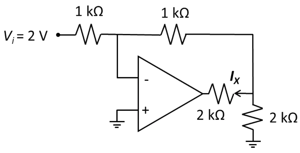
An inverting amplifier has 1 kΩ in, from V, and 1 kΩ of feedback to a node N. N is driven from the op-amp output through 2 kΩ (current , towards the output) and loaded by 2 kΩ to ground. Find .
Full question on page 50 of the official paper (PDF)
Show answerHide answer
Key idea: The virtual ground fixes the feedback current, which fixes N's voltage; then apply KCL at N.
Official answer: C
The inverting input is a virtual ground. The input current 2\text{ V}/1\text{ k}\Omega = 2 mA flows on through the 1 kΩ feedback resistor, so the node at its far end (call it N) sits at
KCL at N: 2 mA arrives through the feedback resistor, and 1 mA arrives from ground through the 2 kΩ load (since N is at -2 V). Both leave through the 2 kΩ towards the op-amp output, in the direction of I_X:
I_X = 2 + \frac{0 - (-2)}{2} = 3\text{ mA}The op-amp output sits at -2 - 3 \times 2 = -8 V. Option (C).
Learn the idea:
GATE 2026, Q.60
Analog Circuits2 marksNAT
An NMOS has its gate tied to its drain, which is fed from V through 1 kΩ ( V, mA/V², no channel-length modulation). Find the gate voltage .
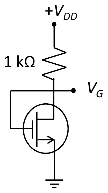
Answer format: Volts, rounded off to two decimal places
Full question on page 56 of the official paper (PDF)
Show answerHide answer
Key idea: A diode-connected MOSFET is always in saturation; equate the resistor and drain currents.
Official answer: 2.50 to 2.60
Call the gate voltage V. Since V_{DS} = V_{GS} > V_{GS} - V_{TH}, the transistor is saturated, and the resistor current equals the drain current (mA, V):
The other root is negative, below threshold, so it's rejected. The drain current is 5 - 2.56 = 2.44 mA. V_G \approx 2.56 V.
GATE 2026, Q.62
Analog Circuits2 marksNAT
An inverting amplifier has at the input and a T network as feedback: from the inverting input to a node, from that node to ground and from it to the output. All four are 50 kΩ. Find the magnitude of the closed-loop gain.
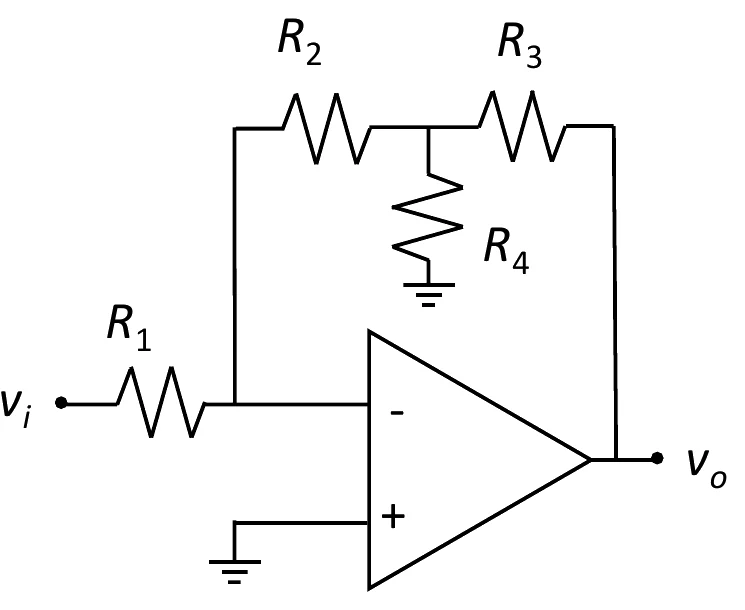
Answer format: A number (the magnitude), rounded off to two decimal places
Full question on page 57 of the official paper (PDF)
Show answerHide answer
Key idea: Find the T's middle-node voltage from the virtual ground, then apply KCL there.
Official answer: 2.90 to 3.10
The inverting input is a virtual ground, so v_i/R_1 flows through R_2 to the T's middle node M:
V_M = -\frac{R_2}{R_1}v_i = -v_iKCL at M: v_i/R_1 arrives through R_2, and R_4 draws V_M/R_4 = -v_i/R_4 (it pushes current in). Both flow on through R_3:
In general the gain is -\tfrac{R_2 + R_3 + R_2R_3/R_4}{R_1}, here -3. The magnitude is 3.00.
Learn the idea:
GATE 2026, Q.65
Analog Circuits2 marksNAT
V drives a 10 kΩ series resistor. At the output, one branch is 10 kΩ and an ideal diode D1 to a +2 V battery; the other is an ideal diode D2 from a V battery. Find the maximum output voltage.
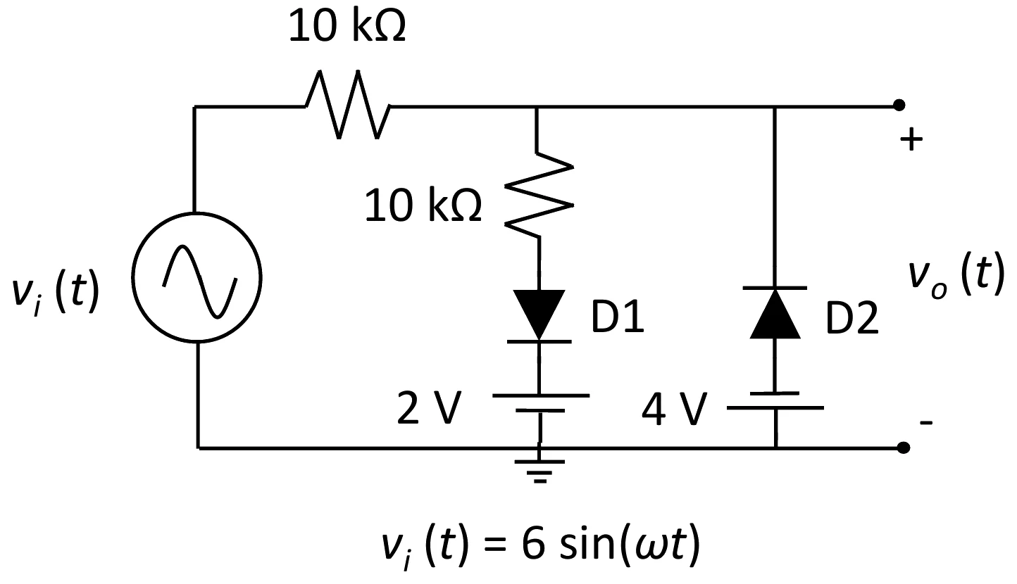
Answer format: Volts, rounded off to two decimal places
Full question on page 58 of the official paper (PDF)
Show answerHide answer
Key idea: On the positive peak D1 conducts and the two 10 kΩ resistors divide between the input and +2 V.
Official answer: 3.70 to 4.30
With no load, the output equals v_i until a diode turns on.
- D1 (anode towards the output, cathode on the +2 V battery) turns on when v_o > 2 V.
- D2 (cathode on the output, anode on the battery's negative side, at -4 V) turns on when v_o < -4 V, so it only clips the negative half.
On the positive peak D1 conducts, and the two 10 kΩ resistors divide between v_i and 2 V:
Learn the idea:
GATE 2025, Q.21
Analog Circuits1 markMCQ
In the small-signal circuit in the figure, drives through , carrying , and a dependent source flows down from the output node, which has to ground. What is the voltage gain ?
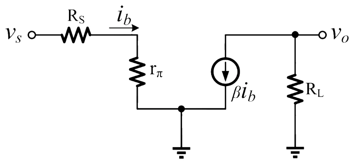
Full question on page 20 of the official paper (PDF)
Show answerHide answer
Key idea: Find i_b from the input loop alone, then let the dependent source drive the load.
Official answer: A
The input side is R_S and r_\pi in series, so
i_b = \frac{v_s}{R_S + r_\pi}The source \beta i_b pulls current down out of the output node, so that current flows up through R_L and makes v_o negative:
Option (A). Dropping r_\pi gives (C), and missing the inversion gives (D).
Learn the idea:
GATE 2025, Q.22
Analog Circuits1 markMCQ
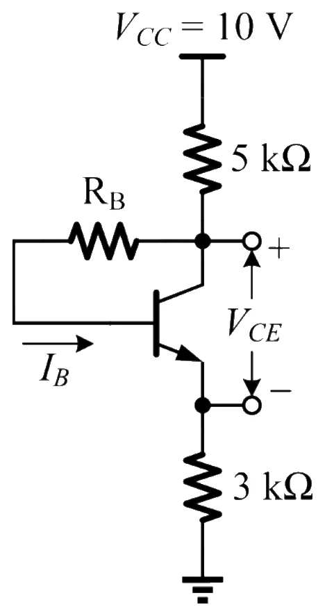
In the circuit in the figure, V feeds the collector through 5 kΩ, the emitter has 3 kΩ to ground, and connects the collector to the base. The ideal BJT is in the active region with . If µA, what is in volts, to two decimal places?
Full question on page 21 of the official paper (PDF)
Show answerHide answer
Key idea: With R_B taken from the collector, the collector resistor carries the base current as well as the collector current.
Official answer: C
With \beta = 100 and I_B = 10 µA, I_C = 1 mA and I_E = 1.01 mA.
The 5 kΩ carries I_C + I_B = 1.01 mA, because I_B leaves the collector node through R_B. So
Option (C). Options (A) and (B) are V_C and V_E on their own, and using only I_C in the 5 kΩ gives 1.97 V.
Learn the idea:
GATE 2025, Q.29
Analog Circuits1 markMSQ
Which statements about an ideal op-amp are TRUE?
One or more options are correct.
Full question on page 28 of the official paper (PDF)
Show answerHide answer
Key idea: An ideal op-amp amplifies only the difference between its inputs, draws no input current and drives any load.
Official answer: A and C
An ideal op-amp has infinite input resistance (A) and infinite differential gain (C). Its output resistance is zero, not infinite, so it can drive any load, and its common-mode gain is zero, since it ignores what the two inputs share (infinite CMRR). Options (A) and (C).
Learn the idea:
GATE 2025, Q.30
Analog Circuits1 markMSQ
For ideal MOSFET single-stage DC-coupled amplifiers with finite load resistors, which statements are TRUE?
One or more options are correct.
Full question on page 28 of the official paper (PDF)
Show answerHide answer
Key idea: Whether the signal goes into the gate or the source decides the input resistance, and which terminal it comes out of decides the phase.
Official answer: B and D
- (A) is false: a common-gate stage takes its input at the source, where the input resistance is about 1/g_m.
- (B) is true: the common-source input is the gate, which draws no current.
- (C) is false: the common-source gain is -g_m R_D, so the output is inverted.
- (D) is true: the common-drain stage (source follower) has a positive gain just under 1.
Options (B) and (D).
GATE 2025, Q.34
Analog Circuits1 markNAT
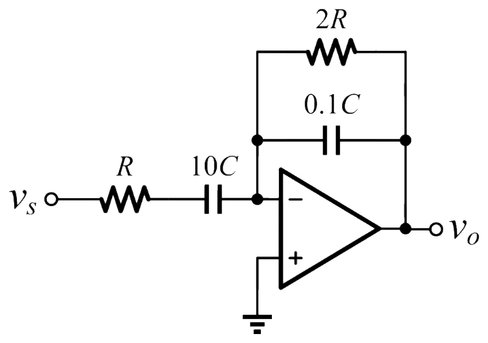
In the ideal inverting filter in the figure, the input is in series with , and the feedback is in parallel with . The lower dB frequency is 1 MHz. What is the upper dB frequency, in MHz?
Answer format: MHz, rounded off to the nearest integer
Full question on page 30 of the official paper (PDF)
Show answerHide answer
Key idea: The input network sets the lower corner and the feedback network the upper one, each through its own time constant.
Official answer: 50
The gain is -Z_f / Z_i, with
\frac{V_o}{V_s} = -\frac{2R}{1 + j\omega(0.2RC)} \cdot \frac{j\omega(10RC)}{1 + j\omega(10RC)}The input network is a high-pass with its corner at 1/(2\pi \cdot 10RC), and the feedback network a low-pass with its corner at 1/(2\pi \cdot 0.2RC). Taking each corner as a -3 dB frequency, their ratio is
Note: The exact -3 dB points come out at about 54 MHz, because the two poles interact (the peak gain is 1.96, not 2). The key uses the standard corner-frequency approximation, which is the method expected in the exam.
Learn the idea:
GATE 2025, Q.43
Analog Circuits2 marksMCQ
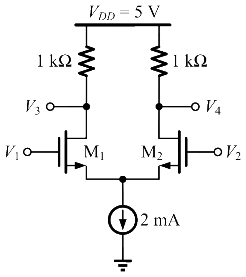
In the differential pair in the figure, the identical ideal MOSFETs and are in saturation with mS. Each drain has 1 kΩ to V, and the tail current is 2 mA. The inputs are and volts. What is , the drain voltage of , in volts?
Full question on page 38 of the official paper (PDF)
Show answerHide answer
Key idea: The tail current splits equally at rest, and each transistor's current changes by g_m times half the differential input.
Official answer: D
At rest each transistor carries half of 2 mA, so V_3 = 5 - 1\,\text{k}\Omega \times 1\,\text{mA} = 4 V.
The differential input is V_1 - V_2 = 0.02\sin\omega t. Each transistor sees half of it, so M_1's current rises by
Option (D). The drain falls when the current rises, hence the minus sign; using the whole differential input gives the 0.1 in (B) and (C).
GATE 2025, Q.47
Analog Circuits2 marksMCQ
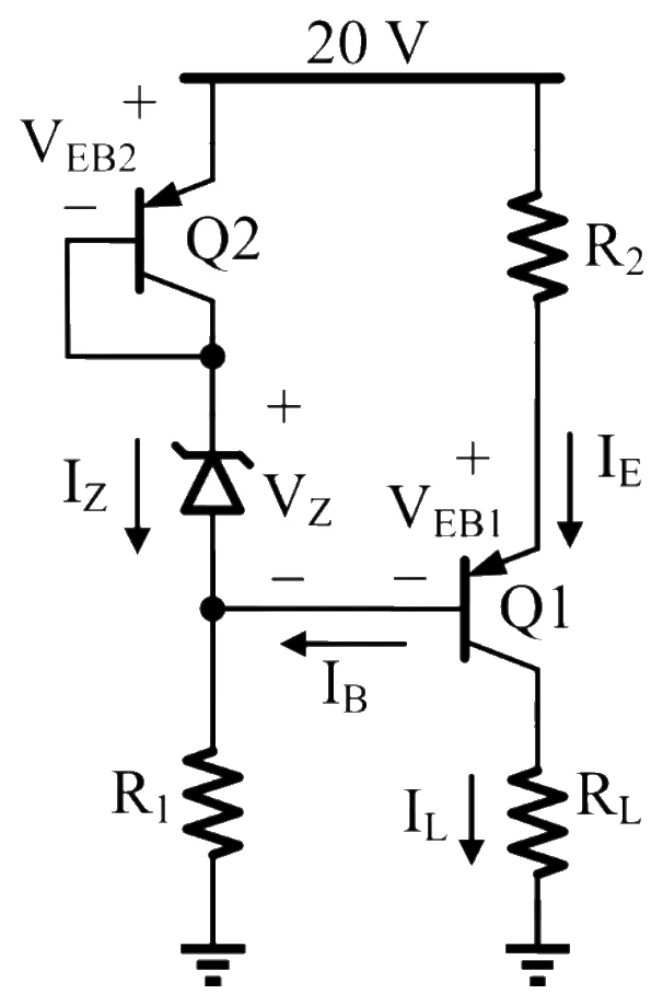
In the circuit in the figure, identical PNP transistors and are active with , and V. is diode-connected from the 20 V rail into a Zener diode in breakdown ( V, mA), which feeds to ground. That node drives 's base; 's emitter has to 20 V and its collector feeds the load. If mA, what are and in kΩ, to one decimal place?
Full question on page 42 of the official paper (PDF)
Show answerHide answer
Key idea: The diode drop and the Zener voltage fix Q_1's base voltage, and the base current adds to the Zener current in R_1.
Official answer: A
Q_2 drops 0.7 V, so the Zener's top is at 19.3 V and its bottom node at 19.3 - 5 = 14.3 V. That node is Q_1's base.
I_L = I_{C1} = 12 mA, so I_B = 12/120 = 0.1 mA and I_E = 12.1 mA. The base current flows out of Q_1's base into the node, joining the Zener current in R_1:
Option (A).
Learn the idea:
GATE 2025, Q.57
Analog Circuits2 marksMSQ
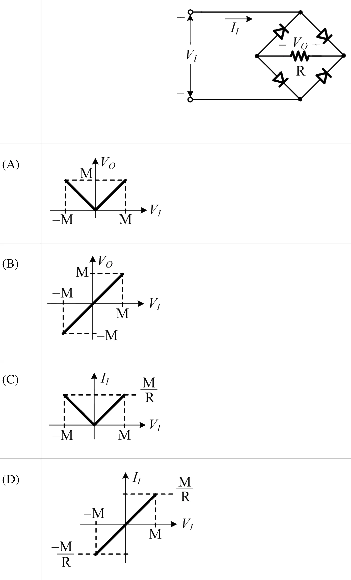
All diodes in the bridge in the figure are ideal, with across the bridge and across . As is swept from to volts, which of the plots (A) to (D) are correct?
One or more options are correct.
Full question on page 49 of the official paper (PDF)
Show answerHide answer
Key idea: A bridge routes current through the load the same way for either input polarity, but the source current still reverses with the source.
Official answer: A and D
For V_I > 0 one pair of opposite diodes conducts, and for V_I < 0 the other pair does. Either way the current through R flows the same way, so V_O = |V_I|: plot (A), not (B).
The source sees R in either case, but its current reverses with V_I: I_I = V_I / R, a straight line from -M/R to M/R. That is plot (D), not (C). Options (A) and (D).
Learn the idea:
GATE 2025, Q.61
Analog Circuits2 marksNAT
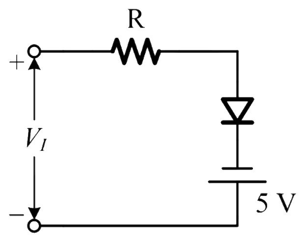
In the circuit in the figure, V drives , an ideal diode and a 5 V battery in series. The battery's negative terminal is joined to the diode's cathode and its positive terminal to the bottom of the input. For how long in each period of the input is the diode forward biased, in ms?
Answer format: ms, rounded off to two decimal places
Full question on page 51 of the official paper (PDF)
Show answerHide answer
Key idea: Read the battery's polarity first: here it pulls the cathode below the input's reference, so the diode conducts for most of the cycle.
Official answer: 13.32 to 13.34
The battery holds the cathode 5 V below the bottom terminal, so the ideal diode conducts whenever V_I > -5 V:
That holds for every \theta except 210° < \theta < 330°: for 240° of each 360°. The period is 2\pi / 100\pi = 20 ms, so
Reading the battery the other way round, with the diode needing V_I > 5 V, gives 6.67 ms.
Learn the idea:
GATE 2024, Q.17
Analog Circuits1 markMCQ
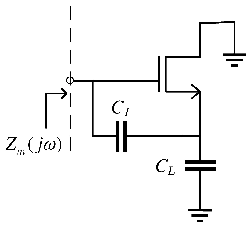
In the circuit in the figure, the long-channel NMOS is in saturation with transconductance ; its drain is at AC ground, joins gate and source, and joins source and ground. Neglecting body effect, channel-length modulation and device capacitances, what is the input impedance at the gate?
Full question on page 15 of the official paper (PDF)
Show answerHide answer
Key idea: Drive a test current into the gate and follow it through C_1 into the source node, where the transistor adds g_m v_{gs}.
Official answer: A
A test current i into the gate flows through C_1, so v_{gs} = i / (j\omega C_1). At the source, i and the drain current g_m v_{gs} both flow into C_L:
Option (A). The real part is negative: this is the negative resistance that sustains a Colpitts oscillator.
GATE 2024, Q.18
Analog Circuits1 markMCQ
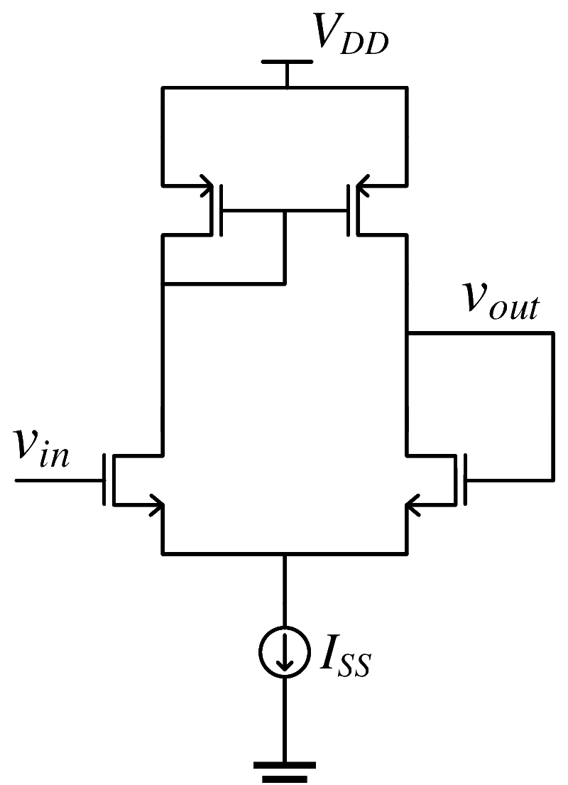
In the closed-loop amplifier in the figure, a MOSFET differential pair with a current-mirror load has its output tied back to the second input, and the magnitude of its open-loop low-frequency gain is 40. With all transistors in saturation, an ideal , and body effect, channel-length modulation and device capacitances neglected, what is the closed-loop gain , to three decimal places?
Full question on page 16 of the official paper (PDF)
Show answerHide answer
Key idea: Feeding the whole output back to the inverting input makes a buffer whose gain is A/(1 + A).
Official answer: A
The output is fed back in full (\beta = 1) to the input that subtracts, so
Option (A). An ideal op-amp would give 1.000, option (B); the finite gain of 40 leaves about a 2.4% shortfall.
Learn the idea:
GATE 2024, Q.23
Analog Circuits1 markMCQ
In the circuit in the figure, an ideal step-down transformer with a centre-tapped secondary feeds the load through two ideal diodes and with no forward drop. If V and the average load voltage is V, what is ?
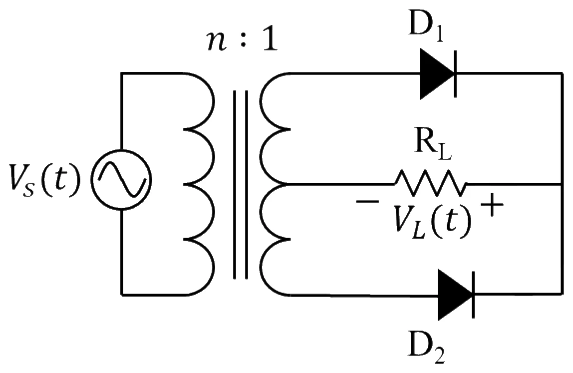
Full question on page 20 of the official paper (PDF)
Show answerHide answer
Key idea: In a centre-tapped full-wave rectifier, each diode sees half the secondary, and the load sees both half-cycles.
Official answer: A
The secondary has a peak of 10/n V, so each half has 5/n V. Full-wave rectification of a peak V_m averages 2V_m/\pi:
Option (A). Taking the whole secondary as each diode's voltage gives 8, option (B).
Learn the idea:
GATE 2024, Q.35
Analog Circuits1 markNAT
In the circuit in the figure, a 10 µF capacitor starts at 10 V. At a switch closes and it discharges through 10 kΩ and an ideal Zener diode with V, reverse biased by the capacitor. What total energy is dissipated in the Zener, in mJ?
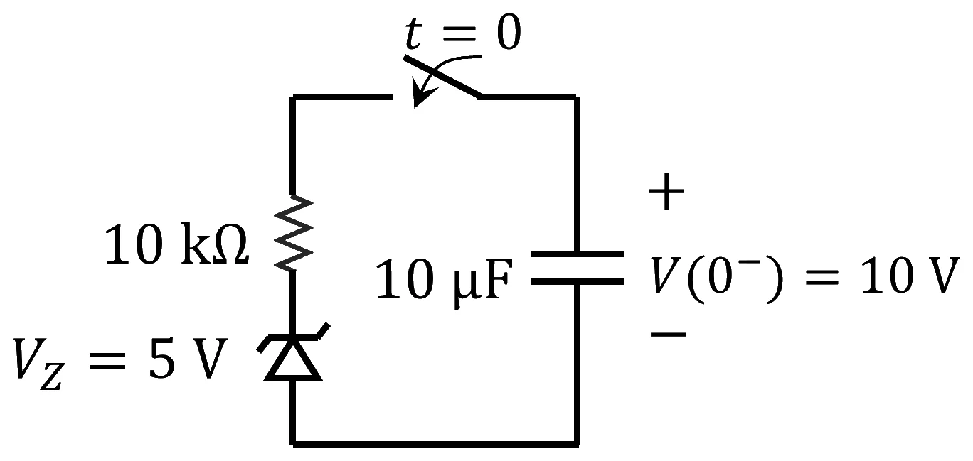
Answer format: mJ, rounded off to three decimal places
Full question on page 26 of the official paper (PDF)
Show answerHide answer
Key idea: An ideal Zener holds exactly V_Z while it conducts, so its energy is V_Z times the charge that passes through it.
Official answer: 0.25
The Zener conducts in breakdown while the capacitor is above 5 V, so the capacitor falls from 10 V to 5 V and then the current stops. The charge that flows is
The capacitor gives up \tfrac{1}{2}C(10^2 - 5^2) = 0.375 mJ; the other 0.125 mJ heats the resistor.
Learn the idea:
GATE 2024, Q.49
Analog Circuits2 marksMCQ
In the circuit in the figure, the ideal op-amps saturate at ±10 V and the inductor current starts at 0. OPA1 is a non-inverting Schmitt trigger with 10 kΩ from and 100 kΩ of positive feedback; its output drives OPA2 through a 1 mH inductor, with 1 kΩ of feedback. is a triangle of ±2 V peak and 8 µs period. Which statement is true?
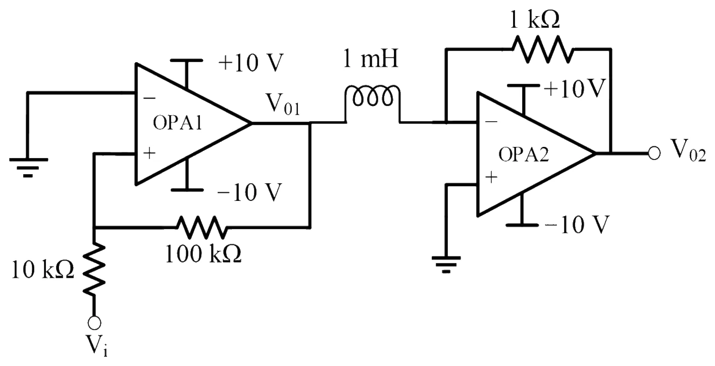
Full question on page 37 of the official paper (PDF)
Show answerHide answer
Key idea: Hysteresis delays each switch until the input reaches a threshold, and an integrator that reaches the rail clips its ramp.
Official answer: D
OPA1 switches when its + input crosses 0, which happens at V_i = \pm 10 \times \frac{10}{100} = \pm 1 V. The triangle changes by 4 V in 4 µs, 1 V/µs, so it reaches 1 V 1 µs after its zero crossing: V_{01} is a ±10 V square wave delayed by 1 µs.
OPA2 with an inductor in and a resistor in feedback is an integrator: V_{02} = -\frac{R}{L}\int V_{01}\,dt. Its ramp rate is \frac{1000}{10^{-3}} \times 10 = 10^7 V/s, so it reaches the 10 V rail in 1 µs, well inside each 4 µs half-period, and stays there:
V_{02} is a trapezoid. Option (D).
Learn the idea:
GATE 2024, Q.50
Analog Circuits2 marksMCQ
In the circuit in the figure, an ideal op-amp is a non-inverting amplifier ( to ground, in feedback), and its output returns to the + input through a network of series , shunt , series and shunt . For sustained oscillation, what are and the frequency?
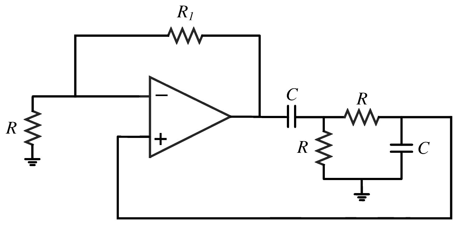
Full question on page 38 of the official paper (PDF)
Show answerHide answer
Key idea: Oscillation needs the loop gain to be exactly 1 at the frequency where the network's phase shift is zero.
Official answer: B
Solving the two-node network with \omega normalised to 1/RC, its transfer is real at \omega = 1/RC, where
\frac{V_{fb}}{V_{out}} = \frac{1}{3}So the amplifier must give exactly 3: 1 + R_1/R = 3, R_1 = 2R, and the frequency is 1/(2\pi RC). Option (B). The 29 and \sqrt{6} in the other options belong to the three-section RC phase-shift oscillator.
Learn the idea:
GATE 2024, Q.51
Analog Circuits2 marksMCQ
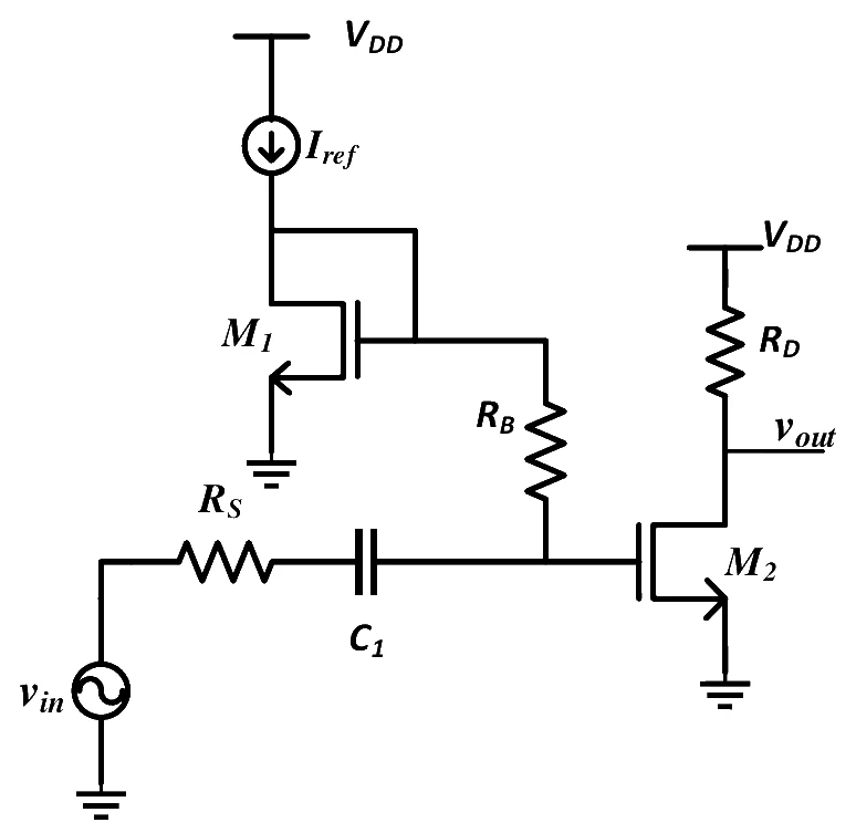
In the circuit in the figure, and are in saturation with transconductances and . is diode-connected under , and joins its gate to the gate of , which drives . The input reaches 's gate through and . Neglecting body effect, channel-length modulation and device capacitances, with a short for AC, what is the exact ?
Full question on page 39 of the official paper (PDF)
Show answerHide answer
Key idea: A diode-connected MOSFET looks like a resistance of 1/g_m to AC, and the ideal current source above it is an open circuit.
Official answer: B
For AC, I_{ref} is open and the diode-connected M_1 is 1/g_{m1} to ground. So M_2's gate sees R_B + 1/g_{m1} to ground, which forms a divider with R_S:
Option (B). Leaving out R_B gives (D), and forgetting the divider altogether gives (A).
GATE 2023, Q.21
Analog Circuits1 markMCQ
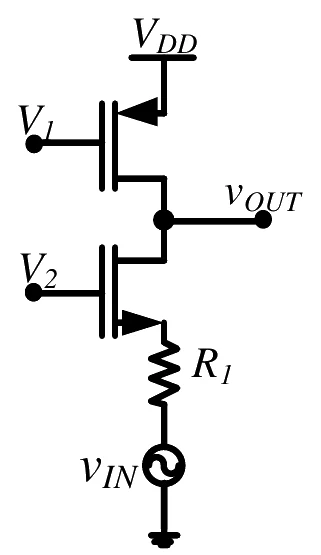
In the circuit in the figure, and are bias voltages. Based on its input and output impedances, the circuit behaves as a
Full question on page 15 of the official paper (PDF)
Show answerHide answer
Key idea: Low input impedance means the input is a current; high output impedance means the output is a current.
Official answer: D
The NMOS is a common-gate stage: its gate is held at V_2 and the signal enters at its source. Looking into a source the impedance is about 1/g_m, which is low, so the stage takes a current as its input.
The output is taken at the drains, where the NMOS drain and the PMOS current source (gate at V_1) both look like high impedances, about r_o each, so the output behaves as a current. Low input impedance and high output impedance make a current controlled current source, a current buffer. Option (D).
GATE 2023, Q.22
Analog Circuits1 markMCQ
A cascade of common-source amplifiers in a unity gain feedback configuration oscillates when
Full question on page 15 of the official paper (PDF)
Show answerHide answer
Key idea: A question given marks to all scores full marks for every candidate, whatever they answered.
Official answer: Marks to all
The key awards marks to all for this question and doesn't say why, so we don't pick an option.
The idea behind it: a feedback amplifier oscillates when the loop gain reaches 1 in magnitude at the frequency where the loop's phase shift makes the feedback positive (the Barkhausen condition). One likely reason for the ruling is that the options state the condition in terms of the closed-loop gain and a strict inequality on the phase, so none of them states the condition exactly.
Ruling in the key: The key gives marks to all (MTA) for this question: every candidate received its 1 mark.
GATE 2023, Q.39
Analog Circuits2 marksMCQ
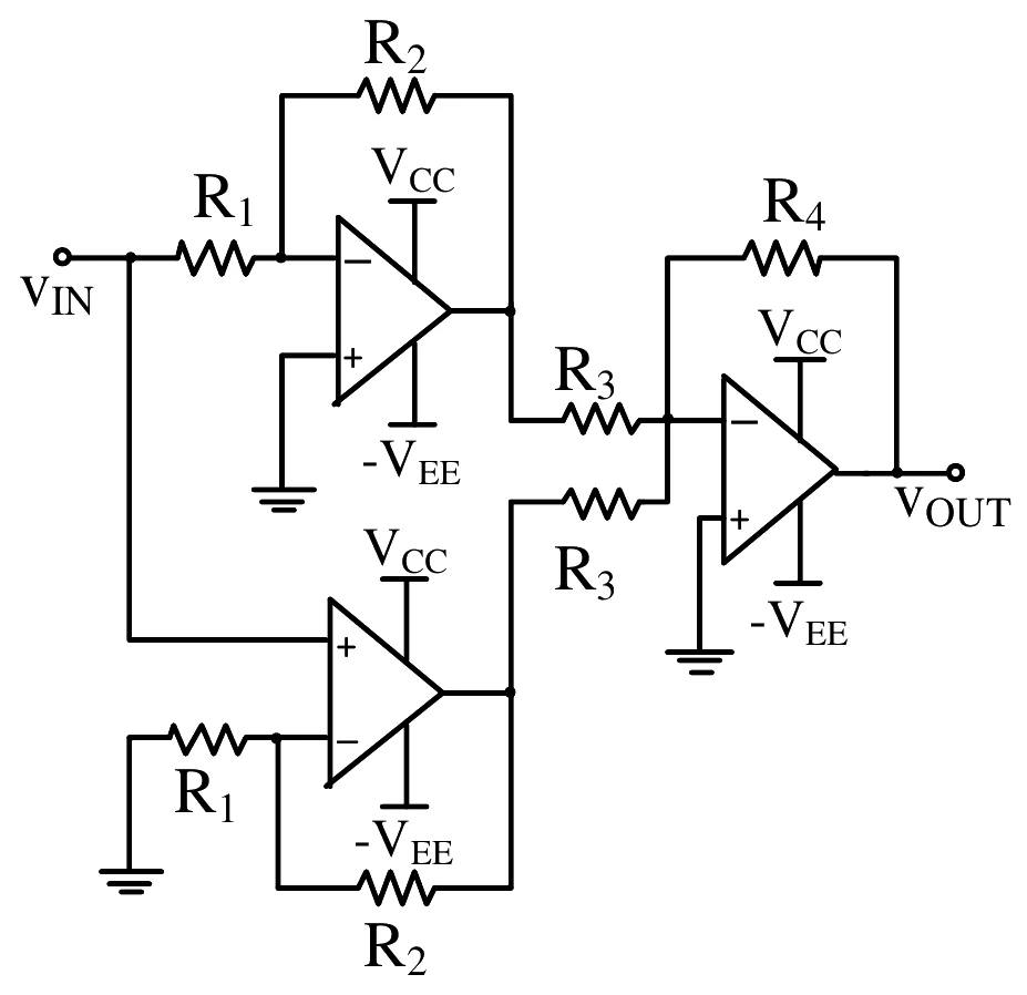
In the circuit in the figure, drives an inverting amplifier (, ) and a non-inverting amplifier (, ); their outputs feed, each through , the inverting input of a third op-amp with feedback and its non-inverting input grounded. What is ?
Full question on page 26 of the official paper (PDF)
Show answerHide answer
Key idea: The third op-amp is an inverting summer, and the first two outputs add to exactly v_{IN}.
Official answer: A
The summer gives v_{OUT} = -\dfrac{R_4}{R_3}(v_1 + v_2) = -\dfrac{R_4}{R_3} v_{IN}. Option (A).
Learn the idea:
GATE 2023, Q.40
Analog Circuits2 marksMCQ
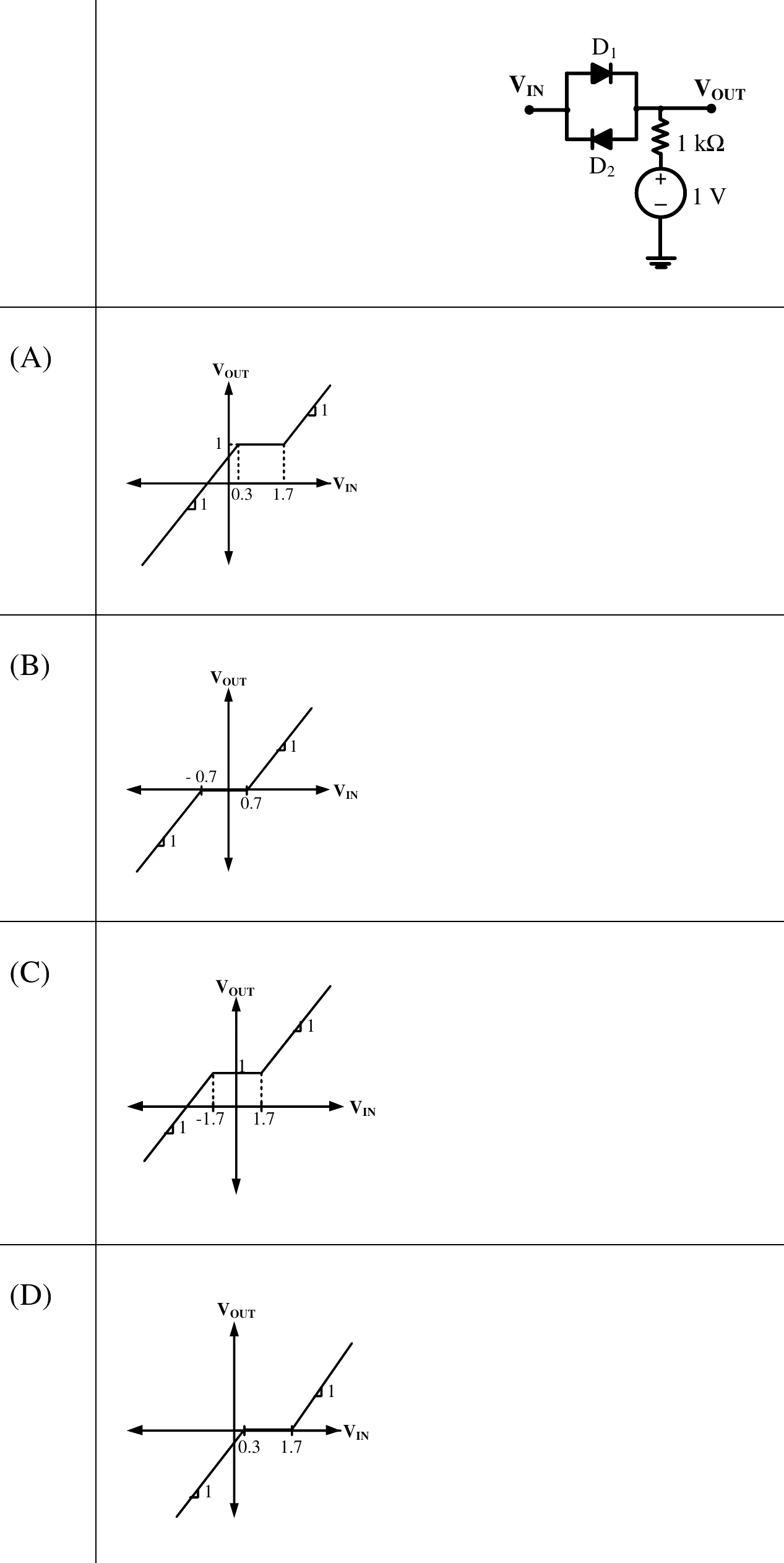
In the circuit in the figure, and are silicon diodes with a cut-in voltage of 0.7 V, connected in anti-parallel between and ; connects through 1 kΩ to a 1 V source. Which transfer characteristic is correct?
Full question on page 27 of the official paper (PDF)
Show answerHide answer
Key idea: With no diode on, no current flows in the 1 kΩ, so V_{OUT} sits at 1 V.
Official answer: A
While |V_{IN} - 1| < 0.7, neither diode conducts, no current flows and V_{OUT} = 1 V: that is 0.3 \le V_{IN} \le 1.7.
For V_{IN} > 1.7, D_1 conducts and V_{OUT} = V_{IN} - 0.7. For V_{IN} < 0.3, D_2 conducts and V_{OUT} = V_{IN} + 0.7. Both have slope 1, joining the flat part at 1 V. Option (A).
Learn the idea:
GATE 2023, Q.64
Analog Circuits2 marksNAT
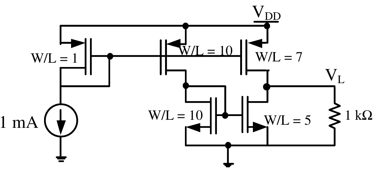
In the circuit in the figure, a 1 mA reference flows through a diode-connected PMOS (W/L = 1). It is mirrored by PMOS devices with W/L = 10 and W/L = 7. The W/L = 10 PMOS feeds a diode-connected NMOS (W/L = 10), which is mirrored by an NMOS with W/L = 5. The output node, where the W/L = 7 PMOS and W/L = 5 NMOS drains meet, drives a 1 kΩ load to ground. What is the voltage , in V?
Answer format: V, rounded off to two decimal places
Full question on page 43 of the official paper (PDF)
Show answerHide answer
Key idea: In saturation, a mirror copies the reference current scaled by the ratio of W/L.
Official answer: 2
- PMOS W/L = 10: 10 \times 1 = 10 mA, into the diode-connected NMOS of W/L = 10.
- NMOS W/L = 5: \tfrac{5}{10} \times 10 = 5 mA, drawn from the output node.
- PMOS W/L = 7: 7 \times 1 = 7 mA, pushed into the output node.
The difference, 7 - 5 = 2 mA, flows through the 1 kΩ, so V_L = 2 \times 1 = 2.00 V, assuming every transistor stays in saturation and channel-length modulation is ignored.